


Abstract
Modern nanotechnology allows the production of, depending on the application, various quantum nanostructures with selected properties. These properties are strongly influenced by the confinement potential which can be modified e.g. by electrical gating. In this paper, we analyze a nanostructure composed of a quantum dot surrounded by a quantum ring. We show that, depending on the details of the confining potential, the electron wave functions can be located in different parts of the structure. Since many properties of such a nanostructure strongly depend on the distribution of the wave functions, by varying the applied gate voltage one can easily control them. In particular, we illustrate the high controllability of the nanostructure by demonstrating how its coherent, optical and conducting properties can be drastically changed by a small modification of the confining potential.

Content from this work may be used under the terms of the Creative Commons Attribution-NonCommercial-ShareAlike 3.0 licence. Any further distribution of this work must maintain attribution to the author(s) and the title of the work, journal citation and DOI.
1. Introduction
Wave function engineering refers to an unprecedented ability to adjust the spatial distribution of the electron wave function in quantum nanostructures through the control of their growth, geometry and electrical fields. It allows us to explore the basic issues of quantum mechanics to design new devices in which some specific properties can be optimized.
Nanotechnology [1, 2] now enables precise control of structural parameters both at the fabrication stage of quantum nanostructures [3, 4] as well as dynamically while operating the device, e.g. through the electrostatic potential [5]. Recent progress allows us to produce complex systems where different building blocks, such as quantum dots (QDs) [6, 7] and quantum rings (QRs) [8], are combined together within a single structure. Such quantum structures are highly relevant to new technologies in which the control and manipulation of electron spin and wave functions play an important role [9]. The potential use of such devices requires, however, deep theoretical analysis.
We have looked for a complex system composed of coupled elements where the coupling constant is an additional parameter that can be controlled by electrical gating. The electronic properties of such a structure can be fine-tuned, which allows monitoring of its properties. In this context, we have performed a comprehensive theoretical analysis of a two-dimensional nanostructure in the form of a QD surrounded by a QR, named afterwards a dot–ring nanostructure (DRN). Such a structure has recently been fabricated by droplet epitaxy [3]. We show that by changing the confinement potential, i.e. the parameters of the potential barrier V0(r) separating the dot from the ring and/or the potential well offset VQD–VQR (see figure 1), one can considerably alter its optical, conducting and coherent properties.

Figure 1. Cross section of the confining potential of a DRN with the marked bottom of the QD potential (VQD), the bottom of the QR potential (VQR), the height of the barrier potential (V0) and the value of the potential outside the DRN (V1). We set VQR = 0. The actual cross sections of the potentials used in calculations are shown in figures 4, 6 and 8.
Download figure:
Standard imageIn particular, we show that by such manipulations one can change:
- (a)the spin relaxation time T1 of DRNs, used as spin qubits or spin memory devices, by orders of magnitude,
- (b)the cross section for frequency selective optical absorption at the microwave and infrared range from strong to negligible,
- (c)the conducting properties of an array of DRNs from highly conducting to insulating.
These features are mostly determined by the so-called overlap factor (OF) (given by equation (3)), which reflects the shape and distribution of the wave functions and can be largely modified by the form of the confinement potential. Thus the microscopic properties of a DRN can be engineered on demand, depending on a particular application.
The paper is organized as follows. In section 2 we present a general theoretical background that will be needed to study particular properties of DRNs. In the following sections we demonstrate, by changing the parameters of the confinement potential, that we can control the spin relaxation time (section 3), the optical absorption (section 4) and the transport properties of DRNs (section 5). The results are summarized in section 6.
2. Basic theoretical formulae
We consider a two-dimensional, circularly symmetric DRN defined by a confinement potential V (r). The DRN is composed of a QD surrounded by a QR and separated from the ring by a potential barrier V0. We assume that the barrier is sufficiently small to allow electron tunnelling between the QD and QR. It ensures that if we change the confining potential at low temperature the electron always occupies the ground state independently of the previous shape of the potential. A cross section of a DRN with explanations of symbols used throughout the text is presented in figure 1.
Such a confinement potential, which conserves the circular symmetry, can be obtained in many ways [1, 10]. Electrostatically defined DRNs can be fabricated, e.g. within a two-dimensional electron gas by placing two gates on the top of it [11, 12]. The gates should have a form of a central circular gate surrounded by a collar gate. The electrons are confined in the quantum well in the regions below the split gates. They can also be constructed by first producing the QD in the two-dimensional electron gas and then performing local oxidation of a narrow circular strip inside it with an atomic force microscope [13]. The electron gas is depleted below the oxidized region thus splitting the structure into the QR with the QD inside. Another method is via droplet epitaxy [3, 14]. The growth procedure is based on the pulsed irradiation of group-V element to group-III element nanoscale droplets at a controlled temperature and fluxes for transforming them into various nanostructures. Droplet epitaxy growth of GaAs allows, through the fine control of As flux and substrate temperature, production of quantum nanostructures with the desired shape, size and dimensionality. It permits combination of QDs and QRs into a single, multifunctional nanostructure, in particular the central QD surrounded by one or more concentric QRs. The discussed structures may also be created by lithography [1, 2].
We start with the confining potential produced solely by electrostatic gating. The electrostatic definition allows one to control and alter the entire potential landscape. In order to make our theoretical results more realistic, the shape of the confinement potential is found by solving the Laplace equation2. Unfortunately, the electrostatically defined nanostructures are relatively large and therefore the resulting relaxation times are small. However, by applying voltage to electrodes one is able to modify the confining potential also in nanostructures produced by means of other methods. In such a case the size of the DRN can be much smaller and we will show that then the relaxation times can be much larger. In order to do that we will assume a smooth confining potential similar to that found from the Laplace equation, but of a smaller diameter.
The most important feature of a DRN is the controllability of the shape of the electron wave functions. The main parameters that affect this shape are the relative positions of the bottoms of the QD and QR confining potentials and the size of the barrier between them. These parameters can be tuned, e.g. by electrical gating. Roughly speaking, if the potential of the QD is much deeper than the potential of the QR, the electrons are located mainly in the QD and the effective size of the wave function is small. On the other hand, if the ring's potential is much deeper the electrons occupy only states in the QR and the wave function is much broader (figure 2). Moreover, by fine-tuning the confinement potential we are able to have, e.g. the ground state located in the QD, with the lowest excited state in the QR (or vice versa). This way we can easily control the OF and all the properties which depend on it. In sections 3 and 4, we show how this feature can be exploited to control relaxation time and optical absorption.

Figure 2. Schematic illustration of the radial part R of the ground state wave function in the case where the QD potential is deeper than the QR potential (left panel) or vice versa (right panel). The solid blue line represents a cross section of the confining potential obtained from the Laplace equation, whereas the dashed red line is a solution of the corresponding Schrödinger equation.
Download figure:
Standard imageAs it was already stated, the confinement potential of the required shape can be produced in many ways. We start with an example of a DRN electrostatically defined by two planar concentric electrodes, a circular one in the center surrounded by a ring-shaped electrode. For such a system we solve the Laplace equations. Depending on the parameters (dimensions and voltages) the resulting potential may smoothly evolve between the limits presented in figure 2. Figure 3 demonstrates the evolution of the potential when the voltage applied to the electrodes is varied. Since our analyses are not limited to electrostatically defined DRNs in calculations we will use a smooth general confining potential of the form proposed in [15, 16]. This potential can be very well fitted to the solution of the Laplace equation, but can describe smaller nanostructures as well. It is important for our analysis that such a potential allows us to study independently the influence of the height of the barrier and the relative position of the bottoms of the potentials of the QR and QD (see figures 4, 6 and 8). In numerical calculations we assume the size of the DRN to be equal to about 160 nm, V1 = 50 meV and we set the zero potential energy at the level of VQR, i.e. the potential well offset is equal to VQD. To be specific, our model calculations are performed for InGaAs systems (with the effective electron mass m* = 0.067me and the electron spin g-factor |gs| = 0.8) for which many theoretical and experimental investigations have been done.

Figure 3. Cross section of the confining potential for different voltages applied to the electrodes.
Download figure:
Standard image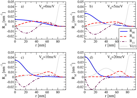
Figure 4. The distribution of the wave functions of the three lowest energy states involved in spin relaxation for different values of V0. VQD = VQR = 0 meV and V1 = 50 meV is assumed.
Download figure:
Standard imageThe single-electron Hamiltonian with the confinement potential V (r) and in the presence of the in-plane magnetic field B is written as

The energy spectrum of H consists of a set of discrete states Enl due to radial motion with radial quantum numbers n = 0,1,2,..., and rotational motion with angular momentum quantum numbers l = 0,±1,±2.... The single-particle wave function is of the form

with the radial part Rnl(r) and the spin part χσ.
For many QDs the energy spectra and the wave functions can be calculated analytically, for other structures have to be calculated numerically. Having given the wave functions one can calculate the OF. It reflects the mutual distribution of the radial parts of any two wave functions in the DRN, and is given by

where n'l' and nl are the quantum numbers of the two energy states involved in the process under investigation. In the following, we consider a DRN occupied by a single electron which couples to photonic (optical absorption) or phononic (spin relaxation) degrees of freedom. For such processes the selection rules allow the electron occupying the ground state to transit/scatter to the states with orbital numbers l = ± 1 only. Then, the relevant OF takes the form

where R00 is the radial part of the ground state wave function (2) and l = ± 1. The second important quantity that depends on confinement and strongly affects absorption and relaxation is the energy gap between the excited orbital and the ground state

The calculated energy levels, modified by electrical gating, will be used in section 3 to estimate the relaxation times for a set of DRNs.
3. Spin relaxation times in dot–ring nanostructures (DRNs)
The spin of a single electron in a circularly symmetric DRN placed in a static magnetic field B with energy levels split by the Zeeman energy ΔZ = gsμBB provides a natural system suitable as a memory device in spintronics and as a qubit in a quantum computer [17]. If kBT ≪ ΔZ ≪ Δ01 then the DRN can be well approximated as a two-level system. The evident goal is to optimize material properties and nanostructure design to achieve long relaxation (and decoherence) times so that sufficient room is left for implementing protocols for spin manipulations and read out.
In our model calculations we assume the in-plane magnetic field B = 1 T (the in-plane orientation is favorable as it does not reduce the distance between the orbital states), thus the Zeeman splitting is equal to ΔZ = 0.046 meV.
It was shown both theoretically [18, 19] and experimentally [5, 20, 21] that the most important spin relaxation mechanism in magnetic fields of the order of a few Tesla is spin–orbit (SO) mediated spin–piezoelectric phonon interaction. The extensive discussion of the relaxation times in QDs and QRs has been also given in [22]. In all these studies it was shown that relaxation times increase strongly with the decrease of the nanostructure radius, so we will not consider this aspect here. We rather focus on the change of T1 governed by the change of the confinement potential that defines the investigated DRN structure.
The formula for the relaxation time T1 governed by the Dresselhaus SO interaction is given by (for detailed derivation see [18]):

Λp is the dimensionless constant depending on the strength of the effective spin–piezoelectric phonon coupling and the magnitude of SO interaction, Λp = 0.007 for GaAs type systems [18, 21]. For a given quantum number n the orbital states with l and −l are degenerated (in a parallel magnetic field), so we take into account only positive values of l multiplying the relevant quantities by a factor of 2. We have checked that for a single electron the relaxation time is determined by the SO coupling to (at most) two lowest excited orbital levels allowed by the selection rules n = 0, l = 1, thus

where

The quantities entering T1 depend on the potential confining the electrons which determines the orbital energy spectrum, the shape of the orbital wave functions and therefore the OF.
Let us first consider a limiting case when VQD = V0 = 0. Then a DRN is a circular QD with radius r0 = 80 nm. The calculated quantities are collected in table 1 (first row) and the corresponding wave functions are presented in figure 4(a). The results show that T1 is entirely determined by the virtual excitation to the first excited orbital state and the reason of small T1 is the relatively large Ξ01. The second allowed excited state (n = 1, l = 1) lies too far in energy to let the electron scatter and the symmetry of the wave function (the dot-dashed line in figure 4(a)) causes a small value of Ξ11. Thus this state does not contribute. It is also seen in figure 5(c) where the relaxation times, calculated independently for transitions 00–01 (T011) and 00–11 (T111), are plotted. The resulting relaxation time of the nanostructure T1 (dot-dashed solid green line in figure 5(c)) for V0 = 0 overlaps with T011. The small value of T1 in this case results from the large radius of the considered QD.

Figure 5. The dependence of the orbital gaps Δnl (a), OFs Ξnl (b), relaxation times (c) and photon absorption cross section (d) on the height of the potential V0. Other parameters (VQD, VQR and V1) are the same as in figure 4. The dot-dashed green line shows the overall relaxation time of the DRN, whereas blue and red lines represent individual relaxation times for phonon coupling to the R01 and R11 states, respectively.
Download figure:
Standard imageTable 1. The values of Δnl, Ξnl, T1 and σi,f as a function of the height of the barrier V0. The parameters are: rQD = 25 nm, rbarrier = 40 nm, rQR = 70 nm, VQD = VQR = 0 meV and V1 = 50 meV.
| V0 | Δ01 (meV) | Δ11 (meV) | Ξ01 (nm) | Ξ11 (nm) | T1 (ms) | σ01 (nm2) | σ11 (nm2) |
|---|---|---|---|---|---|---|---|
| 0 | 0.807 | 3.91 | 5.87 | 0.45 | 0.05 | 6.12 | 0.175 |
| 5 | 1.48 | 3.61 | 3.74 | 1.45 | 0.9 | 4.55 | 1.66 |
| 10 | 2.29 | 4.30 | 1.47 | 2.34 | 18 | 1.1 | 5.16 |
| 15 | 2.85 | 5.26 | 0.53 | 2.30 | 74.2 | 0.18 | 6.13 |
| 20 | 3.26 | 6.12 | 0.20 | 2.16 | 151 | 0.03 | 6.29 |
To get longer T1 small OFs are required and therefore one should take into account a nanostructure in which the wave functions of the ground and first excited orbital states will be separated so that Ξ01 will be very small (while keeping Δ01 reasonably large). It can be done by introducing to a QD a circular potential barrier. When the barrier V0 is present, the structure divides, forming the DRN and the wave function distribution changes drastically (figures 4(b)–(d)). In figures 5(a) and (b), we plotted Δnl and Ξnl respectively as a function of V0, the values are given in table 1. Comparing these figures we see that, in contrast to Ξnl, Δnl changes very little with V0 and it is Ξnl which determines T1. Indeed, when Ξnl increases then Tnl1 decreases and vice versa. For small V0 the dominant contribution to relaxation is given by the state E01 (figure 5(c)). With increasing V0 the wave function of E01 moves over to QR which results in a decrease of Ξ01 (increase of T011) with a simultaneous increase of Ξ11 (decrease of T111). For V0 ≈ 9 meV the contributions to T1 from E01 and E11 are equal and by further increasing the height of the barrier it becomes the higher excited state (E11) that determines T1—a rather unusual situation. A similar effect, recently obtained experimentally by changing the shape of the QD by electrical gating [5], also resulted in an increase of T1 by about an order of magnitude.
To summarize this part, we have shown that by changing the barrier height one can change considerably the relaxation time of DRN by manipulating the orbital energy states and their wave functions.
Similar considerations can be done for DRNs by changing, instead of the barrier height, the potential well offset VQD. Such manipulations can be done experimentally by the application of a disk-shaped potential gate below the QD. For such a setup one can move individual wave functions between the QD and QR (figures 6(a)–(d)) and for sufficiently large values of VQD (positive or negative) we can model the geometry of the nanostructure from QD through DRN to QR. The possible applications of these features will be given in section 5. The results of the calculations of relevant Δs and Ξs are presented in figure 7 and the corresponding relaxation times are given in table 2. We see that within this method one can change T1 in the same range as when manipulating V0 (see T1 in tables 1 and 2).

Figure 6. The distribution of the wave functions of the first three energy states and for different values of VQD. V0 = 15 meV and V1 = 50 meV is assumed.
Download figure:
Standard image
Figure 7. Dependence of the orbital energy gap Δnl (panels (a) and (b)) and OF Ξ (panels (c) and (d)) to the first (panels (a) and (c)) and second (panels (b) and (d)) excited states as a function of VQD for different values of V0.
Download figure:
Standard imageTable 2. The values of Δnl, Ξnl, T1 and σi,f as a function of VQD. The parameters are : rQD = 25 nm, rbarrier = 40 nm, rQR = 70 nm, V0 = 15 meV, VQR = 0 meV and V1 = 50 meV.
| VQD | Δ01 (meV) | Δ11 (meV) | Ξ01 (nm) | Ξ11 (nm) | T1 (ms) | σ01 (nm2) | σ11 (nm2) |
|---|---|---|---|---|---|---|---|
| −9 | 6.73 | 10.3 | 2.07 | 0.03 | 240 | 6.33 | 0.002 |
| −5 | 6.1 | 7 | 2.14 | 0.34 | 150 | 6.15 | 0.18 |
| −2 | 4.45 | 5.65 | 0.54 | 2.20 | 106 | 0.29 | 6.03 |
| 0 | 2.85 | 5.26 | 0.53 | 2.30 | 74.2 | 0.17 | 6.12 |
| 3 | 0.51 | 4.64 | 3.20 | 2.16 | 0.21 | 1.14 | 4.76 |
| 9 | 0.15 | 6.98 | 10.1 | 0.71 | 2×10⁻⁴ | 3.36 | 0.78 |
The increase of T1 is possible even in the limiting case of V0 = 0, i.e. if we manipulate only VQD. It is shown in figures 8(a) and (b) with the resulting relaxation times. This seems to be the simplest possible method to increase T1 by introducing a small disk-shaped gate below a central part of a big QD (without the separating barrier).

Figure 8. Distribution of the radial parts of the electron wave function and the corresponding relaxation time for (a) VQD = −14 meV, (b) VQD = 14 meV.
Download figure:
Standard imageOne should stress that the important feature of such studies is not only the value of T1 itself but the possibility to change it by external conditions which can be steered by electric fields. Besides these long relaxation times have been obtained taking into account only SO mediated interaction with piezoelectric phonons. However other mechanisms of relaxation, (e.g. due to fluctuations of the electric and magnetic field, deformational phonons, multiphonon processes and circuit noise) which we neglected in the above model calculations, can further limit the relaxation time.
In the next section, we discuss another quantity which is determined by the DRN parameters, namely the intraband absorption of microwave and infrared radiation.
4. Engineering the optical absorption of DRNs
The cross section for photon absorption due to electron transition from the ith bound state Ei(ni,li) to the fth bound state Ef(nf,lf) in the dipole approximation is given by the formula [23–25]

where β = 1/137 is the fine structure constant, lf = li ± 1, n2 is the refractive index and FFD(Ei,Ef) ≡ fFD(Ei) − fFD(Ef), with fFD(E) being the Fermi–Dirac distribution function. In these considerations we assume B = 0 and kBT ≪ Δ01. Replacing the delta function by the Lorentzian function with half-width Γ and neglecting the influence of temperature we obtain the maximum cross section at the resonance frequency

With the help of (11) one can analyze the frequency selective absorption for a range of initial and final states. For concreteness we calculate the absorption coefficient from the orbital ground state E00 to the first excited orbital state E01 at frequency ω01 (ℏω01 ≃ Δ01) and to the second excited state E11 at frequency ω11 (ℏω11 ≃ Δ11) and show how it can be modified for different DRNs. Then (11) can be written as

(assuming Γ = 1 meV, n2 = 3.25). The absorption cross sections for the first two optical transitions as a function of the barrier height V0 is shown in figure 5(d). Manipulating V0 we can utilize the on/off switching for absorption of a photon of frequency Δ01/ℏ (Δ11/ℏ). The ratio between on and off cross sections is about 40 (see the last two columns in table 1).
The optical absorption strongly depends also on VQD (figures 9(a)–(d)) for sufficiently large V0. For VQD located much below VQR the wave functions of the ground and first excited state lie in the QD and that of the second excited state in the QR (see e.g. figure 6(a)). It results in a high (small) absorption cross section σ01 (σ11). With decreasing the potential well offset for VQD around –3 meV the distribution of the wave functions changes considerably resulting in σ11 much bigger than σ01. By further increasing VQD the wave functions R00, R01 move over to QR and R11 stays in QD (see e.g. figure 6(d)) which results in a reversed situation. For small V0 these effects are much weaker.

Figure 9. Photon absorption cross section for transition from the ground state to the first (solid blue line) and the second (red dashed line) states as a function of VQD for different values of V0.
Download figure:
Standard imageThese considerations allow us to engineer the DRNs according to their applications:
- (i)one can design DRNs to get the most effective absorption required for efficient infrared and microwave photodetectors, or
- (ii)one can design DRNs with negligible absorption at ℏω01 or ℏω11, i.e. structures which will be transparent for the respective photon frequency.
By changing VQD one can smoothly move over from highly absorbing to almost transparent DRNs. The absorbed photon energy can be changed to a large extent by changing the radius of DRN, the barrier height and the material (e.g. for the structure with m* = 0.04me it changes from microwave to far infrared).
5. The conducting properties of arrays of DRNs
Apart from the unique properties of a single DRN, interesting behaviour emerges when such structures are combined into a two-dimensional array. If they are located sufficiently close to each other, electrons can tunnel from one DRN to another one, making a system that resembles a narrow band crystal. The tunnelling rate depends on the overlap of the electron wave functions on adjoining structures. And since we are able to control the shape of the wave functions, we can control the overlap, and thereby manipulate the transport properties of the crystal-like structure. If the electron wave functions are located in the QDs, the overlap is effectively zero and the system behaves like an insulator. On the other hand, when the wave functions are located in the QRs, the overlap is much larger which results in metallic character. These two situations are illustrated in figure 10.

Figure 10. Electron wave functions in an array of DRNs in the case when electrons are located in the QDs (left panel) and in the QRs (right panel).
Download figure:
Standard imageSince the electronic correlations are not taken into account in our approach, we do not expect a true metal–insulator transition. However, in real nanosystems the Coulomb blockade is present and when the number of electrons per DRN is exactly one (the half-filled case) a Mott-type transition can occur [26]. Then, by changing the gate voltage we would be able to induce the metal–insulator transition. In a finite system, even in the presence of Coulomb correlations, it will not be a phase transition, rather a crossover behaviour between states with localized and itinerant electrons. Such a transition results in a change of the conductance of the array of DRNs. This effect does not require an array consisting of a large number of DRNs: even a single DRN coupled to two leads should have a different conductance depending on the relative position of the bottoms of the QR and QD confining potentials. In the case of two adjoining DRNs the system can be effectively described as a double QD with the coupling controlled by the shape of the confining potential. The conductance of such a system as a function of the inter-dot tunnelling rate has been studied, e.g. in [27]. Similarly, in the case of one-dimensional and two-dimensional arrays of QD the conductance has been studied in [28] and [29], respectively. Note, that in all these systems the Coulomb correlations play an important role.
If we assume that there is a tunnelling between adjoining QRs, but not between adjoining QDs, the array of DRNs can be described by a periodic Anderson-like Hamiltonian [30]
where c†iσ (f†iσ) creates an electron in the ith QR (QD), tij is the transfer energy between adjoining QRs, V describes the hybridisation between states in QD and QR at the same site. In accordance with the Coulomb blockade picture the interaction between electrons in a given QD can be parameterized by a capacitive charging energy UQD = e2/C. Coulomb interaction in QRs is neglected. The difference of the atomic levels  QD − QR can be controlled by the voltage applied to the QD's gates.
There is also another possibility to induce the metal–insulator transition. When a random gate voltage is applied to DRNs an on-diagonal disorder is introduced into the array and the Anderson localization is expected. Controlling individual DRNs in an array may be involved since it requires a supply of voltage to every gate. However, if we are interested only in the global properties of such an array, there is no need to control individual DRNs. In order to be able to control all the DRNs in the same way, i.e. to force electrons to occupy QDs or QRs in all nanostructures, we can place the QDs in one layer and the QRs in another one, located above (or below) the first layer. Then, the difference QD − QR is proportional to the strength of electric field applied to the whole array perpendicularly to the layers. Such configuration is shown in figure 11. Of course, since in this case QDs and QRs are vertically separated, one can use sufficiently large QDs instead of QRs.

Figure 11. Example of a spatial configuration of QR and QD that allows for controlling VQR and VQD by an external electrostatic field.
Download figure:
Standard imageA similar approach has been proposed by Ugajin [31], where an array of coupled QDs was subjected to an external electric field. The QDs were of a convex shape and the applied field moved electrons into the convex portion which led to a larger barrier width between adjacent dots and a smaller transfer energy.
6. Summary
The ability to control the quantum state of a single electron is at the heart of many developments, e.g. in spintronics and quantum computing. In contrast to real atoms, quantum nanostructures allow flexible control over the confinement potential which gives rise to wave function engineering.
In our model calculations we have shown that by manipulating the confinement parameters we can alter the overlap of the electron wave functions so that the transition probability will be enhanced or suppressed on demand. We performed systematic studies of the influence of such manipulations on relaxation times, optical absorption and the conducting properties of DRNs. Thus the basic issues of quantum mechanics can be explored to design new semiconductor devices in which specific properties can be optimized.
The wavelength range of the absorption spectra may be largely expanded from microwave to infra-red by utilizing DRNs of different sizes and different materials. The macroscopic variables such as relaxation time, optical absorption or conductivity can be modified by changing on demand the microscopic features of the nanosystem such as the shape and distribution of the wave functions. Combined quantum structures are highly relevant to new technologies in which the control and manipulations of electron spin and wave functions play an important role. To name a few possible applications, one can imagine tunable or switchable microwave waveguides built with the help of arrays of DRNs with variable optical properties or a single electron transistor based on a single DRN coupled to source and drain leads.
The results indicate a novel opportunity to tune the performance of nanostructures and to optimize their specific properties by means of sophisticated structural design.
Acknowledgments
MMM and MK acknowledge support from the Foundation for Polish Science under the TEAM program for the years 2011–4. EZ acknowledges support from the Ministry of Science and Higher Education (Poland) under grant no. N N202 052940. The authors thank Jerzy Wróbel and Bartłomiej Szafran for valuable discussions.
Footnotes
- 2
The authors are grateful to Bartłomiej Szafran and Michał Nowak for providing the code that was used in this calculation.