


Abstract
The interest in graphene stems from its unique band structure that photoemission spectroscopy can directly probe. However, the preparation method can significantly alter graphene's pristine atomic structure and in turn the photoemission spectroscopy spectra. After a short review of the observed band structure for graphene prepared by various methods, we focus on graphene grown on silicon carbide. The semiconducting single crystalline hexagonal SiC provides a substrate of various dopings, where bulk bands do not interfere with that of graphene. Large sheets of high structural quality flat graphene grow on SiC, which allows the exact same material to be used for fundamental studies and as a platform for scalable electronics. Moreover, a new graphene allotrope (multilayer epitaxial graphene) was discovered to grow on the 4H-SiC C-face by the confinement controlled sublimation method. We will focus on the electronic structure of this new graphene allotrope and its connection to its atomic structure.
Export citation and abstract BibTeX RIS

Content from this work may be used under the terms of the Creative Commons Attribution-NonCommercial-ShareAlike 3.0 licence. Any further distribution of this work must maintain attribution to the author(s) and the title of the work, journal citation and DOI.
1. Introduction
One major technological challenge is to find a new material for the post-silicon CMOS era when Moore's law will end. Carbon nanotubes have remarkable electronic properties (high mobility, robustness, ballistic transport, high current density capability and so on) and are considered a viable candidate for carbon electronics, but the persistent problems with selecting semiconducting or metallic tubes and the inability to accurately place them on a substrate have so far prevented their integration into the electronics industry. Graphene, a two-dimensional honeycomb layer of C atoms, was proposed as an alternative, where multiple interconnected nanostructures could be massively patterned, while retaining the carbon nanotube's essential properties [1].
Despite the progress, graphene is not yet competitive with Si technology. Digital operation requires the presence of a band gap but graphene is a zero-gap semiconductor. While several methods have been proposed (patterning of nanoribbons, or functionalization and chemical doping), a significant and controllable gap is yet to be demonstrated. On the other hand, analogue electronics does not require a band gap and there has been progress towards high-frequency applications. Graphene devices operating at 427 GHz [2] have been demonstrated, and there is, in principle, no limitation for THz operation on a scalable platform such as epitaxial graphene on SiC.
Knowledge of the electronic structure of graphene sheets prepared by a particular method is therefore important for electronic applications. The essential features of the band structure of a carbon honeycomb lattice were first calculated in 1947 [3]. The band structure of graphene is characterized by a linear dispersion around the  point (figure 1), Eph = ℏkvF (where vF is the Fermi velocity), similar to (massless) photons. Electrons do not travel at relativistic velocities since the Fermi velocity is ∼0.003c and therefore
  . However, since two carbon atoms are present in the unit cell (figure 1(a)), electrons have a two-component wavefunction satisfying the Dirac equation, in a formal analogy with relativistic particles [4, 5].
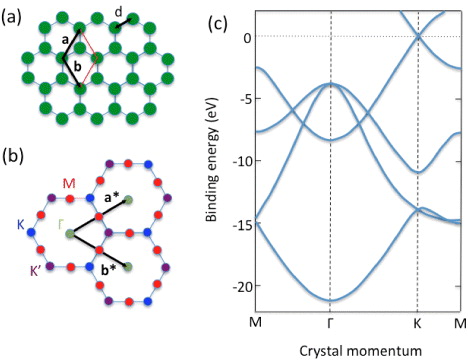
Figure 1. (a) Unit cell of graphene with two atoms, one within the selected unit cell and the other at a corner. The first neighbor distance is d = 1.42 Å. The lattice parameter |a| = 2.46 Å. (b) Reciprocal space for the real space in (a) indicating the high-symmetry points (ΓM = 1.475 Å−1, ΓK = 1.703 Å−1). (c) Band structure calculated by tight binding. Adapted from [6].
Download figure:
Standard imageBecause direct band structure determination is fundamental for understanding graphene's electronic properties, photoemission spectroscopy is key to graphene research. The photoemission technique relies on the detection of photon-excited electrons. When electrons are illuminated with energetic enough photons, they are extracted out of the solid after refraction through the material's surface. Both energy and momentum conservation (parallel to the surface) allow the binding energy and the parallel momentum inside the crystal to be measured. In this way, it is possible to obtain the band structure of graphene. The band structure is very sensitive to different graphene preparations because it is intimately linked to the atomic structure. We will thus review in this paper the observed band structure by photoemission for graphene prepared by different methods. We will pay special attention to SiC, which is an excellent substrate to grow graphene. It can be obtained in large single crystals with atomically flat surfaces, it is insulating but can be doped, and since it is a wide-band gap semiconductor, its bulk bands do not interfere with graphene grown on top. Moreover, a newly discovered graphene allotrope [7], multilayer C-face graphene, can be grown on it by the confinement controlled sublimation method [8]. This fabrication technique produces extended regions of high-quality graphene, well adapted for massive device production, allowing fundamental studies in exactly the same material as that used for applications. We will thus present graphene's electronic properties and their relation to its structure for epitaxial graphene on SiC prepared by the confinement controlled sublimation method.
2. Electronic structure determined by photoemission for various graphene fabrications
The existence of graphene has been known for a long time, even though worldwide interest was only recently awakened. Graphene was first isolated in 1962 by chemical exfoliation [10, 11] and later grown by sublimating Si from SiC [12, 13], or by chemical vapor deposition (CVD) on metallic substrates [14]. In fact, IUPAC specified in 1994 that 'the sufix -ene is used for fused polycyclic aromatic hydrocarbons ...' and recommended that 'a single carbon layer of the graphitic structure can be considered as the final member of this series and the term graphene should therefore be used...' [15]. Since then, many graphene production methods have been developed or improved. Most importantly, graphene grown on a large surface area is relevant for surface science studies: CVD growth on metals [16–22], epitaxy on SiC in ultra-high vacuum [1, 23–27], in an inert atmosphere [28] or in a confined Si atmosphere [8, 29]. Depending on the application, or the research field, a particular graphene production may be more adequate. Epitaxial graphene on SiC is being used for high-performance electronics, while large sheets of graphene produced by CVD on metal and transferred to plastic have potential for cheap flexible and transparent conductors [30]. Chemically exfoliated graphene is useful for supercapacitors. In the following, we will review the main features of the electronic structure obtained by photoemission for different graphene preparations.
2.1. Exfoliated graphene flakes
Mechanically exfoliated graphene flakes on SiO2 have been extensively studied (primarily by transport measurements) due to the ease of preparation. The currently available sample size is adequate for microscopic probing techniques. Figure 2 shows the band structure of exfoliated graphene by microspot angle-resolved photoemission spectroscopy (ARPES) [9] probing a 2 μm diameter region. The data show that the Fermi velocity, in the vicinity of the Dirac point, is 1.09 ± 0.15 × 10⁶ m s−1 in good agreement with the expected value. Photoemission provides more information when analyzing the peak width along momentum distribution curves (profiles of the band structure mapping for a fixed energy, as a function of the crystal momentum k). The experimental width 0.47 Å−1 is a convolution of the intrinsic lifetime of the state as well as extrinsic factors. For this system, the extrinsic factor due to the gradient in the surface normal orientation from rippling of exfoliated graphene when it is placed on the SiO2 substrate dominates the broadening. Knox et al [9] have indeed estimated that a variation of 3° in the surface normal can explain the 0.47 Å−1 experimental width.
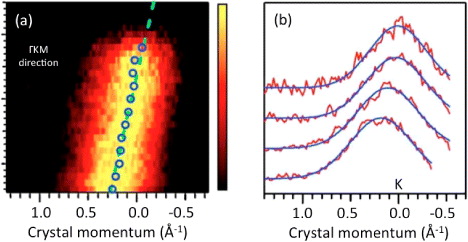
Figure 2. μ-photoemission on an exfoliated graphene flake at hν = 90 eV. (a) Spectral function through the  point along the direction
  . Blue circles correspond to the maxima of the momentum distribution curves and the green line corresponds to the theoretical Fermi velocity. (b) Selected momentum distribution curves in red and the Gaussian fit in blue. Adapted from [9].
Download figure:
Standard image2.2. Graphene on metal surfaces
Graphene can be grown epitaxially on the (111) hexagonal surface of some transition metals. This growth has been studied on Ru(0001) [16–18], Ni(111) [19, 20], Ir(111) [21] or Pt(111) [22]. Graphene in these metals is sometimes characterized by a significant hybridization as in Ni(111) [31] and probably also on Ru(0001) (the graphene–Ru distance is very small and the vibrational and electronic properties of the graphene layer are not those of an isolated graphene sheet [17, 18]). Moreover, since graphene and metals have different in-plane lattice constants and because of the inter-graphene bond stiffness, moiré superperiodicity patterns appear on the surface (figures 3(a) and (b)). For instance, graphene on Ir(111) promotes a moiré pattern with a 2.53 nm lattice parameter in regions of up to a few micrometers.
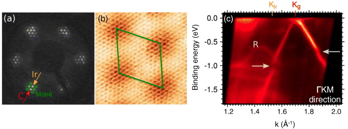
Figure 3. (a) LEED pattern of graphene on Ir(111) at 69 eV. First-order graphene and Ir spots are visible, as well as those corresponding to the moiré pattern at the surface. (b) STM image (5 × 5 nm2, 0.05 V, 32 nA) showing both the graphene unit cell and the superperiodic moiré unit cell. (c) ARPES spectra along the direction  of graphene on Ir(111) (hν = 21.22 eV, 60 K). Minigaps are open due to the strong superperiodic potential. Umklapps of the primary cone are also observed. Adapted from [21].
Download figure:
Standard imageGraphene on Ir(111) grows with its ![$[11\overline {2}0]$](https://content.cld.iop.org/journals/1367-2630/14/12/125007/revision1/nj443184ieqn6.gif) direction aligned with the
direction aligned with the ![$[10\overline {1}]$](https://content.cld.iop.org/journals/1367-2630/14/12/125007/revision1/nj443184ieqn7.gif) direction of the substrate. Measurements along the
direction of the substrate. Measurements along the  direction of graphene correspond to the same symmetry direction of Ir(111). Along this direction, the substrate has a gap around the
  point of graphene, so the electronic properties of the graphene layer can be easily explored. Figure 3 shows a π-band Dirac cone with graphene's characteristic linear dispersion. The full-width at half-maximum of the momentum distribution curve is very narrow (0.035 Å−1), indicating excellent structural quality in the 2 mm region explored by photoemission in this experiment. Moreover, an additional R band appears, which corresponds to the superperiodicity introduced by the moiré pattern. At the intersection of the R band with the primary band, a minigap opens, demonstrating a coupling between graphene and Ru.
2.3. Epitaxial graphene on SiC
From a photoemission perspective, silicon carbide as a substrate for graphene growth has several advantages. Hexagonal SiC has a symmetry well adapted for graphene, and epitaxial graphene growth is observed on 4H- and 6H-SiC. Graphene can be grown both on the Si-face (4H-SiC(0001)) and the C-face (SiC( )), where a truncated bulk crystal ends with Si atoms (C atoms, resp.) exposing a single dangling bond towards the vacuum. SiC is a wide-band gap semiconductor, which allows the growth of adlayers without a significant hybridization to the bulk (C-face). The predicted unperturbed ideal graphene electronic structure was measured for graphene layers on the C-face of 4H-SiC. The surface can be very flat down to a roughness of 50 pm over 0.3 μm [33], with a continuous top graphene layer covering the entire SiC surface. This allows for a k-resolution that is only limited by the instrument resolution. The interface between epitaxial graphene and SiC is formed at high temperature and is therefore ordered and reproducible. This is in contrast with graphene transferred from graphite, where trapped impurities are a major source of scattering and irreproducibility. The interface can also be modified by passivation and intercalation, allowing for multiple functionalities. Silicon carbide can be structured by etching [34] and graphene grows preferentially on the side walls of the trenches. With this directed growth method, thousands of parallel nanoribbons can be grown directly at high temperature with no subsequent etching. These nanostructures have much improved properties compared to etched ribbons [35] and can be readily studied by photoemission. Furthermore, epitaxial graphene on SiC is compatible with mass electronic device fabrication techniques by standard lithographic processes, with no (potentially damaging) transfer required since the growth substrate is a good semiconductor already widely used by the electronic industry. Monocrystalline SiC wafers with diameters up to 150 mm and atomically smooth surfaces that are ready for epitaxial growth are abundantly available (at a price of about $20 cm−2).
Figure 4 compares the band structure of an Si-face substrate that has been annealed at 1150 °C (panel (a)) and at 1250 °C (panel (b)) [32]. The lowest annealing temperature corresponds to a  reconstruction
  in the following) [1, 13], and the highest to the growth of the first graphene layer. Interestingly, the
  exhibits the graphene σ band indicating that C atoms in the last layer are already disposed to the honeycomb lattice of graphene. The Brillouin zone also has the same extension as that of graphene, so the bond length of the C atoms must be that of graphene. It is also observed that the σ bands are shifted by 1.0 ± 0.1 eV towards higher binding energies with respect to graphite, whereas in graphene (figure 4(b)) the shift is only 0.4 eV due to a partial filling of the σ* bands due to substrate doping. Finally, the
  surface does not develop the π band. This C layer thus has a similar structure to graphene but does not have its characteristic linear dispersion. Such a layer is called a zero-layer or 'buffer' layer. The absence of the pz bonds helps to decouple the graphene layer that grows above the buffer layer, which interacts through van der Waals forces [13].
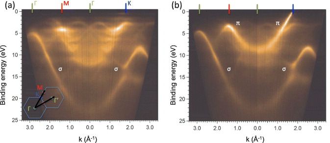
Figure 4. Overall band structure along Γ00MΓ10 and Γ00KM measured by ARPES with hν = 50 eV of (a) the buffer layer on SiC(0001), which exhibits a  reconstruction and (b) 1 ML of graphene on top of the previous substrate. Insets show the directions on the reciprocal space where the measurements are made. Adapted from [32].
Download figure:
Standard imageGraphene on the buffer layer of the Si face of SiC has the characteristic cones at the  points of reciprocal space. Figure 5(a) shows a constant energy cut of the band structure for a binding energy of –1.45 eV, where six cones appear around the six K points, as well as six replicas, corresponding to diffraction of photoemitted electrons through the
  reconstruction. The cone intensity is not homogeneous, because photoemission matrix elements suppress the spectral weight in the outermost part of the cone along the
  direction [6]. This intensity suppression is called 'dark corridor' [37] and it appears due to the interference of the two graphene sublattices in photoemission intensity [37–39]. As the initial state of the photoemission process is a linear combination of pZ orbitals located on A and B atoms, |ψi〉 = α|pz,A〉 ± β|pz,B〉 (with β/α = A eiθk) and the photoemission intensity according to Fermi's Golden Rule is I∝|〈ψf|Hint|ψi〉|2 where Hint is the interaction Hamiltonian, then the photocurrent is [37]

where ϕ0 is the phase difference between electrons emitted from atoms A and B. The second factor |〈ψf|Hint|pz〉|2 depends on the experimental geometry and on the final state effects, so it varies with photon energy or polarization effects. The first factor describes the suppression of intensity in the 'dark corridor' [37–39] and it appears due to the sublattice interference. This term is responsible for the fact that cuts of the electronic structure along two orthogonal directions, as indicated in figure 5(a), will have qualitatively different features (figures 5(b) and (c)) when one of them goes through the 'dark corridor'.

Figure 5. Electronic properties of 1 ML graphene grown on 6H-SiC(0001). (a) Constant energy cut of the band structure at a binding energy of ED–1 eV, i.e. –1.45 eV. The spectral weight is not equivalent when crossing the  point along the
  direction or perpendicularly. (b) Band dispersion across the
  point along the
  direction for an intrinsically doped graphene monolayer. (c) Band dispersion taken across the
  point, in a perpendicular direction to that in (b). Adapted from [36].
Download figure:
Standard imageThe overall band structure follows the expectations from tight binding calculations, with a hopping energy of 2.82 eV, except for a 0.45 eV shift of the Dirac point below the Fermi level that can be understood as graphene electron doping by the depletion of SiC [36]. Other deviations from the expected ideal graphene dispersion appear when looking more carefully at the Dirac point region (figures 5(b) and (c)). Firstly, there is a kink at ∼200 meV below the Fermi level attributed to the electron–phonon coupling [36]. Secondly, linear extrapolations of the bands below the Dirac point do not pass through the bands above. Early studies have attributed the distorted spectral features near the Dirac point to a gap at the Dirac point [40, 41] originating from graphene–substrate interactions [42]. Further studies have shown that the features near ED could also be due to many-body effects [24, 43–45]. Figure 5(c) shows that another kink appears near the Dirac point and is responsible for the apparent mismatch of the upper and lower cones in figure 5(b). This kink has been attributed to electron–plasmon coupling [36].
Another interesting point is the behavior of the graphene layers stacked on the Si face of hexagonal SiC [46]. The interaction between stacked layers increases the number of observed π bands because the Bernal stacking makes the two C atoms within the graphene unit cell non-equivalent and lifts the degeneracy at  .
.
Graphene also grows on the (111) surface of cubic SiC (which has a hexagonal symmetry). This has been demonstrated by the linear band dispersion measured in ARPES (figure 6(b)) as well as other experimental techniques [25]. Graphene can also be grown on the (001) surface of cubic SiC, which has a square surface lattice. Here again, the growth of graphene is demonstrated by its linear band dispersion (figure 6(a)). Moreover, the growth of graphene on cubic SiC must decouple significantly graphene and the substrate owing to the large lattice mismatch between the two [23].
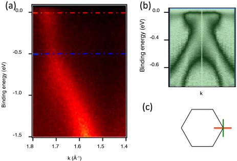
Figure 6. Band structure near EF of graphene grown on cubic silicon carbide (3C-SiC(111)) in two different preparations. (a) Si-rich SiC(001) exposed to a series of annealing cycles with increasing the temperature from 1200 to 1550 K. Adapted from [23]. (b) SiC(111) surface first annealed under Si flux at 900° to remove the native oxide and further annealed from 900 to 1200° to develop the graphene layer. Adapted from [25]. (c) Brillouin zone and measurement direction for (a) in red and for (b) in green.
Download figure:
Standard image3. Epitaxial graphene on C-face
3.1. Atomic structure
Studies of epitaxial graphene on the C-face of silicon carbide SiC(000 ) were initially neglected because LEED patterns suggested it to be disordered. Figure 7 compares the LEED patterns of graphene on the Si- and on the C-face. The Si-face shows a clear LEED pattern where the
  spots are evident, while on the C-face the intensity is spread on small angle arcs. X-ray diffraction (XRD) and STM images both rule out that the angular dispersion originates from small graphite flakes with different orientations on the surface; instead they clearly demonstrate that the dispersion comes from large stacked layers with different relative orientations within the stack.

Figure 7. LEED patterns of (a) 6H-SiC(0001) (Si-face) and (b) 6H-SiC( ) (C-face).
Download figure:
Standard imageFigure 8 shows the STM images of graphene grown on both faces of silicon carbide. STM on Si-face graphene exhibits an apparent 6 × 6 symmetry due to the rippling of the surface, which is more pronounced than the  . On the other hand, the C-face graphene shows different moiré patterns (figure 9(a)). These moiré patterns are caused by commensurate layers rotated by an angle θ that gives rise to a new periodicity at the surface. A commensurate graphene rotation appears when a linear combination of the lattice vectors of one layer ma + nb is equal to a linear combination of the rotated vectors m'eiθa + n'eiθb, with m,n,m' and n' integers. This is satisfied whenever cos θ(m,n) = (4mn + n2 + m2)/2(m2 + n2 + mn), where θ = 0° corresponds to AA stacking and θ = 60° to AB stacking. The new periodicity is defined by the reciprocal vectors


where g1 and g2 are the reciprocal vectors associated with the layer defined by a, b and c = m2 + n2 + mn. Since the two rotated layers are commensurate, a linear combination of G1 and G2 connects their  points (figure 9(b)). Photoemission should observe the characteristic cones of graphene at the K points of each layer, and also the replicas related to the main cones by linear combinations of the supercell reciprocal vectors. Figure 9(c) shows k-PEEM data where such replicas are explicitly visible in a constant energy cut of the electronic structure at 1.3 eV. Umklapps can also be observed in the E(k) representations of photoemitted intensity. Figure 9(d) shows clearly the rotated cones coming from two stacked layers and a replica due to the global periodicity.
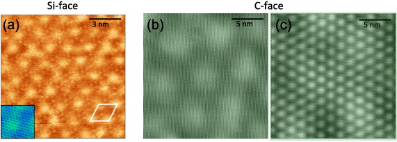
Figure 8. STM images of epitaxial graphene on SiC. (a) Graphene on 6H-SiC(0001) (12 × 12 nm2, –0.2 V, 0.1 nA). The unit cell indicates the apparent (6 × 6) reconstruction. Inset of 2.5 × 2.5 nm2. Adapted from [47]. (b) Graphene on 6H-SiC( ) (20 × 20 nm2, –0.25 V, 0.1 nA, 13 mK). The moiré pattern of 5.7 nm corresponds to a rotation of 2.3° between the two topmost layers. Adapted from [48]. (c) Graphene on 6H-SiC(
 ) with a moiré pattern corresponding to a rotation of 7.34° between the two topmost layers. Adapted from [49].
Download figure:
Standard image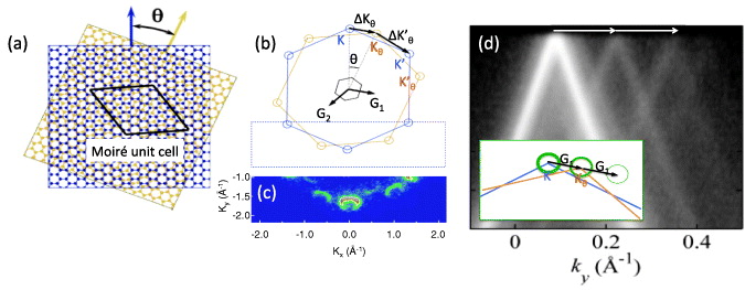
Figure 9. Moiré patterns in graphene on C-face SiC. (a) Real space: two graphene planes rotated by an angle θ give rise to a moiré pattern, with a larger unit cell. (b) Brillouin zones of both rotated planes (blue and orange).  and
and  are symmetry points of the last layer.
  and
and  are symmetry points of the layer underneath. The Brillouin zone of the moiré pattern is indicated in black, with its
  and
and  reciprocal vectors. (c) Constant energy cut at 1.3 eV binding energy of the band structure obtained with a k-PEEM. Adapted from [50]. (d) ARPES data near the
  point. The grayscale is logarithmic to appreciate the weakest features. Three cones related by the moiré reciprocal vector are observed: the two most intense coming from the two last graphene layers and the third one corresponding to a replica with the moiré periodicity. The inset shows a schema of the reciprocal space with three cones related by
  . Adapted from [49].
Download figure:
Standard imageThe rotation angles of the stacked layers have been studied by photoemission and XRD. While the sample is nominally a ten-layer film as determined by ellipsometry, we have localized a thicker region to analyze more stacked layers. These local variations of thickness are inherent to the growth process for films thicker than four layers [52]. In order to analyze the same layer with both photoemission and XRD, we must realize that when XRD gives a diffraction spot at  , the same layer will give rise in photoemission to a conical band at
  , i.e. 30° away from the XRD spot (figure 10(c)). Figures 10(d) and (e) show the histograms as a function of the direction for the conical dispersions in photoemission (figures 10(a) and (b)) and for the diffraction spots in XRD. As shown, both techniques find the same angular distribution of rotated layers. Half of them appear distributed around the
 ![$[21\overline {3}0]$](https://content.cld.iop.org/journals/1367-2630/14/12/125007/revision1/nj443184ieqn42.gif) direction of SiC and the other half 30° away from it, probably indicating that the adjacent layers are rotated on average by about 30° [7], instead of the 60° rotation in graphite. It is important to note that the stacked layers are not rotated by random angles, but alternate 0° ± ∼2 and 30° rotation azimuthally.
direction of SiC and the other half 30° away from it, probably indicating that the adjacent layers are rotated on average by about 30° [7], instead of the 60° rotation in graphite. It is important to note that the stacked layers are not rotated by random angles, but alternate 0° ± ∼2 and 30° rotation azimuthally.
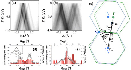
Figure 10. Photoemission intensity at k = 1.704 Å−1 (the  distance) for a nominally ten-layer graphene film (hν = 36 eV) at azimuthal angles (a)
 ![$\alpha _{\mathrm { PES}} =0^{\circ } ([21\overline {3}0])$](https://content.cld.iop.org/journals/1367-2630/14/12/125007/revision1/nj443184ieqn44.gif) and (b)
and (b) ![$\alpha _{\mathrm { PES}} = 30^{\circ } ([10\overline {1}0])$](https://content.cld.iop.org/journals/1367-2630/14/12/125007/revision1/nj443184ieqn45.gif) . (c) Schematic diagram of reciprocal space indicating how to compare angles in XRD with ARPES experiments. Cones in photoemission appear at the
. (c) Schematic diagram of reciprocal space indicating how to compare angles in XRD with ARPES experiments. Cones in photoemission appear at the  point, whereas diffraction spots appear around
  . (d) Comparison of the XRD intensity as a function of the azimuthal angle ϕXRD with the number of cones in photoemission as a function of αPES. Adapted from [51].
Download figure:
Standard imageIn other graphene fabrication methods (specifically higher temperature growth methods), grains with different crystallographic orientations appear in different regions of the sample, as observed by LEEM [53]. When the LEEM aperture is 400 nm, only the diffraction spots corresponding to a single layer are observed but when it is increased to 5 μm, other diffraction spots appear at different angles. In confinement-controlled sublimation graphene, there are also some spatial domains as observed by STM [33]. However, the situation is different from that of [53], as STM clearly shows the presence of stacked layers by direct observation of the moiré pattern (figure 8). Moreover, photoemission reflects the long-range order of these stacked layers as the umklapps due to the rotated-layers moiré periodicity are observed (figure 9(b)).
Finally, the simulation of XRD data unambiguously discards a major contribution of grains with different crystallographic orientations in confinement-controlled sublimation graphene. Figure 11 compares experimental XRD data with a calculation of the graphene (10L) rod intensities assuming grains with Bernal stacking with those from rotationally stacked layers [51, 54]. The comparison of the latter with the experimental crystal truncation rod (CTR) excludes an important contribution of different grains to the diffraction signal when probing regions of 1 mm2. All these results converge to the conclusion that C-face graphene grown by confinement-controlled sublimation has a mostly ordered rotational stacking.
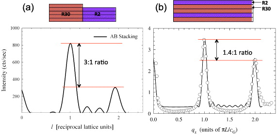
Figure 11. SXRD CTR (10L). (a) Simulation for independent AB stacked domains. (b) Comparison of the experimental SXRD CTR (10L) from a 30-layer C-face graphene film with a random stacking model. Adapted from [51].
Download figure:
Standard image3.2. Ideality of dispersion
Photoemission can explore directly the electronic structure of epitaxial graphene because it has a well-defined surface normal. Figure 12 shows the electronic dispersion of 11 layers of graphene grown on the C-face of SiC. Not all layers are visible due to the limited mean free path of the escaping electrons. This makes approximately half of them appear on the ![$[10\overline {1}0]$](https://content.cld.iop.org/journals/1367-2630/14/12/125007/revision1/nj443184ieqn48.gif) direction shown here. The three visible cones have a clear linear dispersion and their Dirac point is almost at the Fermi level. The Dirac point energy varies from sample to sample, from +33 meV (p-doped) to –14 meV (n-doped). This doping is very small, probably because the observed layers are far from the SiC substrate that charges graphene at the interface. Finally, we observe that most of the cones do not show the parabolic dispersion of graphite, indicating that very few graphene layers are Bernal stacked (figure 12(b)). Because the degeneracy lifting of the two bands in the
direction shown here. The three visible cones have a clear linear dispersion and their Dirac point is almost at the Fermi level. The Dirac point energy varies from sample to sample, from +33 meV (p-doped) to –14 meV (n-doped). This doping is very small, probably because the observed layers are far from the SiC substrate that charges graphene at the interface. Finally, we observe that most of the cones do not show the parabolic dispersion of graphite, indicating that very few graphene layers are Bernal stacked (figure 12(b)). Because the degeneracy lifting of the two bands in the  point (figure 13(a)) due to Bernal stacking is easily identified, we can carry out a detailed statistical analysis. These studies show that less than 15% of the layers are Bernal stacked in these samples. Therefore, we conclude that the original stacking of graphene on C-face SiC preserves the ideal dispersion of a single layer of graphene.

Figure 12. (a) The first direct observation of the ideal dispersion on graphene (epitaxial graphene, C-face). The dotted line indicates the energy where the profile at the bottom has been performed to better observe three cones due to stacked graphene sheets. The inset shows the explored region in reciprocal space. Adapted from [55]. (b) Photoemission intensity of graphite (hν = 83 eV), superimposed on LDA and GW calculations. The parabolic band dispersion is evident, as well as a second band with a maximum around –0.6 eV. Adapted from [31].
Download figure:
Standard image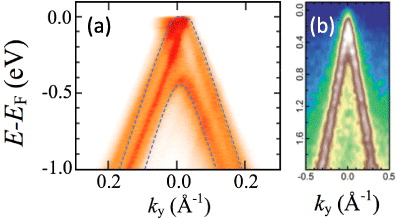
Figure 13. Graphene on SiC, C-face. (a) Multilayer sample. Photoemission data (hν = 36 eV, 40 μm spot) in a selected region showing AB stacking, as denoted by the two parabolic bands highlighted by the dotted lines corresponding to a tight binding dispersion. Adapted from [51]. (b) Three-monolayer sample. Photoemission data on the sample observed by k-PEEM (figure 9(c)). Adapted from [50].
Download figure:
Standard imageFigure 12 shows no gap opening at the crossing points of the different cones. A gap would be indicative of an interaction between adjacent layers. Calculations do not predict an interaction [7, 56, 57], although others predict a coupling between two stacked rotated layers [58, 59]. The coupling is expected to lead to an explicit Fermi velocity renormalization as well as gap opening at the crossing point between two cones from adjacent rotated layers, giving rise to a van Hove singularity (figure 14).

Figure 14. (a) Graphene cones of two independent graphene layers. (b) Velocity renormalization due to interlayer coupling. (c) van Hove singularity of interacting graphene layers. Adapted from [49].
Download figure:
Standard imageThe Fermi velocity renormalization (slower velocities) and a predicted van Hove singularity should induce a large distortion of the ideal dispersion for small rotation angles of adjacent layers near the crossing point of the two cones [58, 59]. We have thus looked at photoemission for Dirac cone dispersions separated by small angles (i.e. figure 9). One must first check that the observed cones are not originating from different regions of the surface and that they come from rotationally stacked layers. We have thus analyzed pairs of cones that satisfy two conditions: (i) they are related by a vector G1 that also connects a third replica of the moiré periodicity (which probes the commensurate relation between the considered cones) and (ii) their intensities decrease progressively (as is expected for stacked layers due to the electron mean free path). The Fermi velocities are shown in figure 15. We have analyzed a large number of cone pairs that appear rotated by small angles on different samples. It is possible that some of the analyzed cones might correspond to non-adjacent stacked layers, or pairs with their adjacent layer turned by ∼30° with respect to the visible one in the detection window. In this case, two non-adjacent layers do not interact and no deviation from the ideal dispersion should appear. However, due to the statistical analysis that we have performed, some of the analyzed cones must correspond to adjacent layers. We find that none of the observed cones (with the exception of Bernal stacked pairs) show a renormalized Fermi velocity. The absence of Fermi velocity renormalization obtained by photoemission in an averaged surface of microns is fully consistent with the observations of STM.

Figure 15. (a) Comparison of the measured (vF) and predicted renormalized ( ) Fermi velocities. Measurements consist of photoemission [49] and STM data [48]. Predictions consist of tight binding [59] and full tight binding calculations [58]. The dashed line is the average Fermi velocity for all the measured cones in photoemission. (b) Two cones that originated at two graphene layers with 1.7° relative rotation. The dashed line is the predicted van Hove singularity from a continuum tight binding model [59]. Adapted from [49].
Download figure:
Standard imageSTM directly identifies adjacent sheets by viewing their moiré patterns. Moiré patterns corresponding to a 2.3° relative rotation have a Fermi velocity of 1.08 ± 0.03 × 10⁶ m s−1 as extracted from Landau level [48] positions. Finally, macroscopic probing techniques such as infrared measurements also do not find a Fermi velocity renormalization [60]. These results are different from the calculations that predict the Fermi velocity renormalization at small rotation angles. Moreover, the data are not consistent with the van Hove singularity scenario of [59] (figure 15(b)), as experimental points do not fit with the predictions. It is possible that some observed points do not correspond to adjacent layers. In this case, it is normal that no interaction is present, i.e. no van Hove singularity or no Fermi velocity renormalization is observed. Another explanation for the inconsistency between different theories and experimental data came with the work of Mele [61]. Mele showed that a missing symmetry in graphene bilayers with a small relative rotation angle allows two states to appear in the coupled system. One of these states renormalizes its Fermi velocity as predicted in some of the theories, while the Fermi velocity renormalization of the other state is prevented by a pseudospin selection rule. This state might correspond to the observation in multilayer epitaxial graphene.
In conclusion, we have demonstrated in this review that the properties of graphene depend on both the growth method and how graphene is stacked or coupled to its support substrate. We have then reviewed the unique properties of graphene grown on the C-face of SiC, i.e. SiC( , when grown by the confinement-controlled sublimation method in an RF furnace. This fabrication method gives rise to stacked graphene layers as observed by moiré patterns in STM, which probes unambiguously the presence of stacked rotated commensurate layers. Photoemission observes umklapp processes associated with the periodicity of the moiré pattern. This work confirms that C-face graphene grown by the confinement-controlled sublimation process is rotationally stacked and does not correspond to different spatial domains. More interestingly, photoemission has observed directly the linear dispersion of the bands of each of these layers. For the top layers of a stack, no distortion is observed, and the doping is extremely small, so each of the stacked layers behaves like a single ideal graphene layer.
Acknowledgments
This research was supported by the W M Keck Foundation, the Partner University Fund from the Embassy of France and the NSF under grant numbers DMR-0820382 and DMR-1005880. We also acknowledge the SOLEIL synchrotron radiation facilities and the CASSIOPEE beamline.