Abstract
We show that weak antilocalization by disorder competes with resonant Andreev reflection from a Majorana zero mode to produce a zero-voltage conductance peak of order e2/h in a superconducting nanowire. The phase conjugation needed for quantum interference to survive a disorder average is provided by particle–hole symmetry—in the absence of time-reversal symmetry and without requiring a topologically nontrivial phase. We identify methods of distinguishing the Majorana resonance from the weak antilocalization effect.
Export citation and abstract BibTeX RIS

Content from this work may be used under the terms of the Creative Commons Attribution-NonCommercial-ShareAlike 3.0 licence. Any further distribution of this work must maintain attribution to the author(s) and the title of the work, journal citation and DOI.
GENERAL SCIENTIFIC SUMMARY Introduction and background. The search for Majorana fermions (particles that are their own antiparticles) in superconducting nanowires has focused on the detection of conductance peaks at zero voltage. The experiments are performed in a magnetic field, and it was generally believed that this would suppress conductance peaks of a more mundane origin, such as the weak antilocalization effect. Indeed, in metals the systematic interference of time reversed paths that is responsible for this effect is incompatible with a magnetic field.
Main results. In this paper, we point out that in the presence of a superconductor weak antilocalization can coexist with a magnetic field. This was actually first noticed in the 1990s, but the implications for the Majorana experiments had been overlooked. Computer simulations show that the conductance peak from weak antilocalization can be deceptively similar to a Majorana resonance.
Wider implications. The conductance peak is not a 'smoking gun signature' of Majorana fermions. It is quite possible to eliminate weak antilocalization as an explanation, but it cannot be ruled out categorically. We are promoting the 'half integer conductance quantization' as an alternative probe of these elusive quasiparticles.
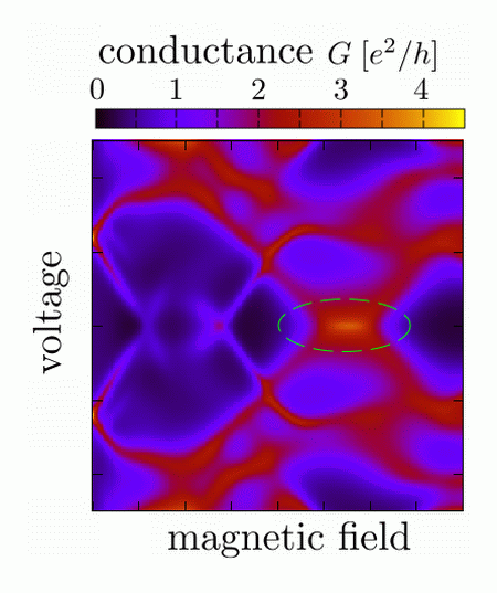 Figure. Computer simulation of the conductance of a superconducting nanowire. A conductance peak at zero voltage appears (encircled), without Majorana fermions.
1. Introduction
Weak localization (or antilocalization) is the systematic constructive (or destructive) interference of phase conjugate series of scattering events. In disordered metals it is time-reversal symmetry that provides for phase conjugation of backscattered electrons and protects their interference from averaging out to zero [1, 2]. A magnetic field breaks time-reversal symmetry, changing the disorder-averaged conductance by an amount δG of order e2/h. The sign of δG distinguishes weak localization (δG < 0, conductance dip) from weak antilocalization (δG > 0, conductance peak).
Andreev reflection at a superconductor provides an alternative mechanism for phase conjugation due to particle–hole symmetry. No time-reversal symmetry is needed, so weak (anti)localization can coexist with a magnetic field and is only destroyed by a bias voltage [3, 4]. The resulting zero-bias anomaly in the conductance of a normal-metal–superconductor (NS) junction is obscured in zero magnetic field by the much larger effects of induced superconductivity, which scale with the number of transverse modes N in the junction. These order Ne2/h effects are suppressed by a magnetic field; only the order e2/h effect from weak (anti)localization remains [5].
In a superconducting nanowire, there is an altogether different origin of zero-bias anomalies in a magnetic field, namely the midgap state that appears at the NS interface following a topological phase transition [6–8]4. Resonant Andreev reflection from the zero mode gives a 2e2/h conductance peak at zero voltage [9]. The first reports [10–12] of this signature of a Majorana fermion are generating much excitement [13]. There is an urgent need to understand the effects of disorder in order to determine whether it may produce low-lying resonances that obscure the Majorana resonance [14–18].
These recent developments have motivated us to investigate the interplay of Majorana zero modes and weak (anti)localization. Earlier studies of weak (anti)localization at an NS junction [3, 4, 19–21] did not consider the possibility of a topologically nontrivial phase with Majorana fermions. Calculations of the local density of states near a zero mode [22–24] address the same physics of midgap quantum interference that we do, but cannot determine the conductance.
This paper consists of two parts. Firstly, in section 2 we give a simple model of a disordered NS interface that allows us to obtain analytical results for δG with and without Majorana zero modes. We then turn in section 3 to a numerical simulation of a Majorana nanowire and compare the conductance peak due to weak antilocalization (in the topologically trivial phase) with that from a Majorana zero mode (in the nontrivial phase). The two effects can appear strikingly similar, but in the concluding section 4 we will discuss several ways in which they may be distinguished.
Before we present our findings, we wish to emphasize that it is not the purpose of this work to diminish the significance of experiments reporting the discovery of Majorana fermions in superconductors. In contrast, we feel that existing [10–12] and forthcoming experiments will gain in significance if possible alternative mechanisms for zero-voltage conductance peaks in a magnetic field are identified and understood, so that they can be ruled out. Weak antilocalization was so far overlooked as one such mechanism.
2. Analytical theory
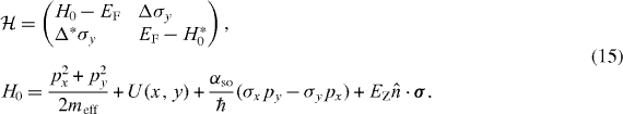
For the analytical calculation we consider a superconducting wire that supports Q topologically protected zero modes at the interface with a normal metal (see figure 1). The stability of Majorana zero modes depends crucially on the fundamental symmetries of the system [25]. At most a single zero mode is topologically protected if both time-reversal symmetry is broken (by a magnetic field) and spin–rotation symmetry is broken (by spin–orbit coupling), so that only particle–hole symmetry remains. This is called symmetry class D with Q∈{0,1}. If the wire is sufficiently narrow (relative to the spin–orbit coupling length), an approximate chiral symmetry [26]5 stabilizes up to N zero modes. (The integer N is the number of propagating electronic modes through the wire in the normal state, counting both spin and orbital degrees of freedom.) This is called symmetry class BDI with Q∈{0,1,2,...,N}.

Figure 1. A bias voltage V0 applied to the normal metal (N) drives a current I into the grounded superconductor (S). Electrons and holes (e,h) are scattered by disorder or a tunnel barrier in N and converted into each other by Andreev reflection at the NS interface, as described by the scattering matrices SN and rA. Particle–hole symmetry ensures that the phase shifts accumulated by e and h along a closed trajectory cancel, irrespective of whether time-reversal symmetry is broken or not. Such phase conjugate series of scattering events permit weak (anti)localization to persist in a magnetic field.
Download figure:
Standard image2.1. Scattering matrix
We construct the scattering matrix of the NS junction at the Fermi level by assuming a spatial separation of normal scattering in N and Andreev reflection in S. Within the excitation gap there is no transmission through the superconductor. The matrix rA of Andreev reflection amplitudes from the superconductor is then a 2N × 2N unitary matrix. Mode mixing at the NS interface can be incorporated into the scattering matrix SN of the normal region, so we need not include it in rA. It has the block form [27, 28]

We have defined ζ = 0 if the difference N − Q is even and ζ = 1 if N − Q is odd, so that N − Q − ζ ≡ 2M is an even integer. The Andreev reflection eigenvalues ρm = sin2αm that are not pinned at 0 or 1 are twofold degenerate [29]6.
The symbols  denote, respectively, an n × n unit matrix or null matrix for n ⩾ 1. The empty set is intended for n = 0. To make the notation more explicit, we give some examples of the direct sums,
The normal region has a scattering matrix

The electron and hole blocks (with N × N reflection and transmission matrices r,r',t,t') are each other's complex conjugate at the Fermi level. The off-diagonal blocks of SN vanish, because the normal metal cannot mix electrons and holes. The matrix s0 is unitary, s0s†0 = 1, without further restrictions in class D. In class BDI, chiral symmetry requires that s0 = sT0 is also a symmetric matrix.
To separate the mixing of modes from backscattering, we make use of the polar decomposition

The matrices U,V,U' and V ' are N × N unitary matrices and  is a diagonal matrix of transmission eigenvalues of the normal region. In class BDI, chiral symmetry relates U' = UT, V ' = VT.
2.2. Conductance
We combine SN and rA to obtain the matrix rhe of Andreev reflection amplitudes (from electron e to hole h) of the entire system. This calculation is much simplified in the case of ζ = 0, ρm = 1 (m = 1,2,...,M) that all modes at the NS interface are Andreev reflected with unit probability. For this case Γ = 0, N − Q = 2M, we obtain

The notation σ⊕My signifies the 2M × 2M matrix constructed as the direct sum of M Pauli matrices.
The Andreev reflection matrix determines the conductance

Substitution of the polar decomposition (4) gives the compact expression

This is the zero-temperature conductance at the Fermi level, in the limit of zero bias voltage. Away from the Fermi level particle–hole symmetry is broken, so the electron and hole blocks in SN are distinct unitary matrices se and sh. If the bias voltage V0 remains small compared to the excitation gap, we can keep the same rA. The finite-voltage differential conductance  is then given by

The electron matrices are evaluated at energy eV0 above the Fermi level and the hole matrices at energy −eV0 below the Fermi level. Chiral symmetry remains operative away from the Fermi level; hence V 'e = VTe, V 'h = VTh ⇒Ωh = Ω†e in class BDI. We will apply equation (8) to voltages large compared to the Thouless energy, when the electron and hole matrices may be considered to be statistically independent.
2.3. Random matrix average
Isotropic mixing of the modes by scattering in the normal region means that the unitary matrices in the polar decomposition (4) are uniformly distributed in the unitary group  . We can calculate the average conductance for a given set of transmission eigenvalues by integration over
  with the uniform (Haar) measure. A full average would then still require an average over the Tn's, but if these are dominated by a tunnel barrier they will fluctuate a little and the partial average over the unitary matrices is already informative.
The calculation is easiest if all Tn's have the same value 0 ⩽ T ⩽ 1. The average zero-voltage conductance 〈G〉 is then given by the integral

with  the density on the unit circle of the eigenvalues eiϕn of ΩΩ*. The corresponding finite-voltage expression has a uniform ρ = N/2π, leading to

irrespective of the symmetry class and independent of the topological quantum number Q.
The zero-voltage average (9) does depend on Q and is different for class D and BDI. The calculations are given in the appendix. Explicit expressions in class D are
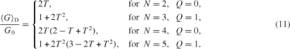
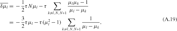
The Q dependence appears to second order in the reflection probability R = 1 − T, while the general first-order result

is Q independent. The corresponding expressions in class BDI are more lengthy, and we only record the small-R result

to show that it is Q-dependent already to first order in R. These are all finite-N results. In the large-N limit the Q dependence is lost,

irrespective of the symmetry class.
As illustrated in figure 2, for the case when all Tn's have the same value T the difference 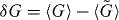 is positive, corresponding to weak antilocalization and a conductance peak. The sign of the effect may change if the Tn's are very different, in particular, in class BDI—which has δG < 0 in a quantum dot geometry (circular ensemble) [28]. It is a special feature of quantum interference in a magnetic field that the distinction between weak localization and antilocalization is not uniquely determined by the symmetry class [21, 31, 32].

Figure 2. Amplitude δG of the average zero-voltage conductance peak as a function of (mode-independent) transmission probability T, in symmetry class D (thick curves) and BDI (thin curves) for different numbers of modes N. The superconductor is topologically trivial when N is even (Q = 0, dashed curves) and nontrivial when N is odd (Q = 1, solid curves). The dash-dotted curve is the Q-independent large-N limit (14).
Download figure:
Standard image3. Simulation of a microscopic model
The random-matrix calculation serves the purpose of a qualitative understanding of the weak antilocalization effect. For a quantitative description we need to relax the assumption of channel-independent Tn's. For that purpose we now turn to a microscopic model of a Majorana nanowire.
3.1. Model Hamiltonian
Following [6, 7], we consider a conducting channel parallel to the x-axis on a substrate in the x–y-plane (width W and Fermi energy EF), in a magnetic field B (orientation  and Zeeman energy
  ), with Rashba spin–orbit coupling (characteristic energy Eso = meffα2so/ℏ2 and length lso = ℏ2/meffαso) and induced s-wave superconductivity (excitation gap Δ0). The Hamiltonian is
The electrostatic potential U = Ugate + δU contains the gate potential Ugate that creates the tunnel barrier and the impurity potential δU that varies randomly from site to site on a square lattice (lattice constant a), distributed uniformly in the interval (−Udisorder,Udisorder). The disordered region is −LN < x < LS, an NS interface is constructed by increasing the pair potential Δ from 0 to Δ0 at x = 0 and a rectangular barrier of height Ubarrier, thickness δLbarrier is placed at x = −xbarrier. The conductance of the normal region (x < 0) contains a contribution Gdisorder from disorder and Gbarrier from the barrier.
The orientation of the magnetic field plays an important role [6, 7]: it lies in the x–y-plane to eliminate orbital effects on the superconductor and we will only include its effect on the electron spin (through the Zeeman energy). A topologically nontrivial phase needs a nonzero excitation gap for EZ > Δ0, which requires a parallel magnetic field B∥ ( ). We will consider that case in the next subsection and then discuss the case of a perpendicular magnetic field B⊥ (
 in section 3.3.
3.2. Average versus sample-specific conductance
To avoid the complications from chiral symmetry, we first focus on a relatively wide junction, W = 3 lso, when symmetry class D (rather than BDI) applies [28]. (We turn to class BDI in the next subsection.) The normal region has N = 8 propagating modes (including spin) in zero magnetic field, for EF = 12 Eso. The topological quantum number Q was determined both from the determinant of the reflection matrix [33]7 and independently by counting the gap closings and reopenings upon increasing the magnetic field. A transition from Q = 0 to 1 is realized by increasing B∥ at fixed Δ0 = 8 Eso.
The results are shown in figure 3 (solid curves) for two geometries, one with the tunnel barrier far from the NS and another with the barrier close to the interface8.
The disorder-averaged conductance shows a zero-voltage peak in a magnetic field, regardless of whether the nanowire is topologically trivial (Q = 0) or nontrivial (Q = 1). The peak disappears in zero magnetic field and instead a conductance minimum develops, indicative of an induced superconducting minigap in the normal region. The two geometries in panels 3(a) and (b) show comparable results, the main difference being a broadening of the zero-bias peak when the tunnel barrier is brought closer to the NS interface—as expected from the increase in Thouless energy9. The shallow maximum which develops around zero voltage in the B = 0 curve of panel 3(b) is a precursor of the reflectionless tunneling peak, which appears in full strength when the barrier is placed at the NS interface [5].

Figure 3. Disorder-averaged differential conductance as a function of bias voltage, for a nanowire modeled by Hamiltonian (15). The two panels (a) and (b) correspond to the two geometries shown to scale above each plot. (The solid vertical line indicates the position of the tunnel barrier, relative to the NS interface; disordered regions are dotted.) Each panel shows data for zero magnetic field (black) and for two nonzero magnetic field values (blue and red). The solid curves are for a parallel field B∥ and the dashed curves for a perpendicular field B⊥. The system is topologically trivial (Q = 0) in all the cases except for the red solid curves (Q = 1).8
Download figure:
Standard image
Figure 4. Numerical simulation of a nanowire for a single disorder realization (no averaging). The color scale gives the differential conductance as a function of bias voltage (the vertical axis) and parallel magnetic field (the horizontal axis). The parameters in panels (a) and (b) correspond to those in figures 3(a) and (b), as listed in footnote 8. The magnetic field range in both panels is in the topologically trivial phase (Q = 0), but still exhibits a conductance peak pinned to zero voltage (green circle).
Download figure:
Standard imageAll this applies to the average conductance in an ensemble of disordered nanowires. Individual members of the ensemble show mesoscopic, sample-specific conductance fluctuations, in addition to the systematic weak antilocalization effect. For some disorder realizations the zero-voltage conductance peak remains clearly visible, see figure 4. The peak sticks to zero bias voltage over a relatively wide magnetic field range, even though the superconductor is topologically trivial (Q = 0). The appearance and disappearance of the peak are not associated with the closing and reopening of an excitation gap, so it cannot produce Majorana fermions [34]10.
3.3. Parallel versus perpendicular magnetic field
So far we have considered a class D nanowire with a magnetic field B∥ parallel to the wire axis. In a perpendicular magnetic field B⊥ (perpendicular to the wire in the plane of the substrate) the symmetry class remains D (broken time-reversal and spin–rotation symmetry), although the topologically nontrivial phase disappears [6, 7]. We therefore expect the class D zero-bias peak to persist in a perpendicular field as a result of the weak antilocalization effect.
This expectation is borne out by the computer simulations, see the dashed curves in figure 3. A zero-bias peak exists for both B⊥ and B∥. If the nanowire is topologically trivial, there is not much difference in peak height for the two magnetic field directions (compare the blue solid and dashed curves). In contrast, if the nanowire is topologically nontrivial for a parallel field, then the peak is much reduced in a perpendicular field (red solid versus dashed curves). The disappearance of the Majorana zero mode and the collapse of the zero-bias peak may be accompanied by the appearance of propagating modes in the superconducting part of the nanowire. This explains the increased background conductance in the red dashed curve of figure 3(a).
The effect of a magnetic field rotation is entirely different when W ≲ lso and the symmetry class is BDI rather than D [26, 28]. The term σxpy in the Hamiltonian (15) can then be neglected, so that  commutes with σy in a perpendicular magnetic field (
 ). The two spin components along
  decouple and for each spin component separately the particle–hole symmetry is broken. We therefore expect both the Majorana resonance and the weak antilocalization peak to disappear in a perpendicular magnetic field for sufficiently narrow wires.
This is demonstrated by the computer simulations shown in figure 5, for the average conductance in a topologically trivial wire of width W = 0.3 lso. The main difference with the data in figure 3 is that the symmetry class is now BDI rather than D, because of the narrower wire. This change of symmetry class does not significantly affect the weak antilocalization peak in a parallel magnetic field. But if the magnetic field is rotated to a perpendicular direction, the peak disappears—as expected for a class BDI nanowire.

Figure 5. The same as figure 3, but now for a narrower wire in symmetry class BDI (rather than D). The system is topologically trivial, without Majorana zero modes. The weak antilocalization peak vanishes if the magnetic field is rotated from B∥ to B⊥.11
Download figure:
Standard image3.4. Effects of thermal averaging
All the results presented so far are in the zero-temperature limit. We calculate the temperature dependence of the differential conductance from the finite-T0 and finite-V0 generalization of equation (6),


Thermal averaging at a nonzero temperature T0 broadens the conductance peak around V0 = 0 and reduces its height, at constant area  under the peak.
This effect of thermal averaging applies to both the weak antilocalization peak and the Majorana resonance, but the characteristic temperature scale is different, as shown in figure 6. The Majorana zero mode is more sensitive to thermal averaging because it is more tightly bound to the NS interface, with a smaller Thouless energy and therefore a smaller characteristic temperature.

Figure 6. Temperature dependence of the conductance peaks from figure 3(b). The four blue curves (Q = 0, topologically trivial) correspond from top to bottom to four increasing temperatures and likewise the four red curves (Q = 1, topologically nontrivial).
Download figure:
Standard image4. Discussion
In conclusion, we have shown that random quantum interference by disorder in a superconducting nanowire can systematically produce a zero-voltage conductance peak in the absence of time-reversal symmetry. This weak antilocalization effect relies on the same particle–hole symmetry that protects the Majorana zero mode, but it exists in both the topologically trivial and nontrivial phases of the superconductor. A conclusive demonstration of Majorana fermions will need to rule out this alternative mechanism for a conductance peak.
There are several strategies one might follow for this purpose:
- Increasing the tunnel barrier with a gate voltage suppresses the weak antilocalization effect, but not the Majorana resonance. The resonance does become narrower, so at finite temperatures thermal smearing will still lead to a suppression with increasing barrier height and this might not be the most effective strategy to distinguish the two effects.
- The disappearance of the conductance peak when the magnetic field is rotated (in the plane of the substrate) towards a direction perpendicular to the wire, the technique used in [10, 12], can identify the Majorana zero mode—but only if the ratio W/lso is sufficiently large that the wire is in class D rather than BDI. In class BDI the Zeeman energy in the rotated field commutes with the Rashba energy, precluding the weak antilocalization effect as well as the Majorana resonance. Both the works [10, 12] have W ≲ lso and are believed to be in class BDI [16, 26], so this complication seems quite relevant.
- Measuring the conductance through a single-mode point contact is a very effective strategy: for N = 1 the zero-temperature conductance G = Q × 2e2/h directly measures the topological quantum number even without any tunnel barrier [35], and this signature of a Majorana zero mode is quite robust against finite temperatures. (The chararacteristic energy scale is the induced superconducting gap in the region between the point contact and the superconductor.) The single mode in the point contact should be spin resolved for this to work: if instead the point contact transmits both spins in one orbital mode (N = 2), then the ambiguity between weak antilocalization and the Majorana resonance remains (see figure 7).
- The Majorana resonance from a wire of finite length should split into two at the lowest temperatures, because of the nonzero overlap of the zero modes at the two ends of the wire [12]. No such systematic splitting will occur for the weak antilocalization peak.

Figure 7. Differential conductance for a single disorder realization of a nanowire (N = 2 spin-resolved modes)12. The left panel shows the appearance of a zero-voltage peak in a range of magnetic field values, for B parallel to the wire. The right panel shows the dependence on the orientation of the magnetic field, for a fixed field strength (EZ = 10 Eso). The zero-voltage peak vanishes if B is perpendicular to the wire. This is the same phenomenology as for a Majorana resonance, but here it happens in the topologically trivial phase.
Download figure:
Standard imageAcknowledgments
We have benefited from discussions with A R Akhmerov and Yu V Nazarov. Numerical simulations of the nanowire were performed with the kwant software package, developed by A R Akhmerov, C W Groth, X Waintal and M Wimmer. This research was supported by the Dutch Science Foundation (NWO/FOM) and by an ERC Advanced Investigator grant.
Appendix.: Random-matrix theory
To evaluate the average conductance (9) we seek the density of the eigenvalues xn = eiϕn of the product X = ΩΩ* of the unitary matrix Ω and its complex conjugate. We denote μn = cosϕn∈[ − 1,1] and determine the joint probability distribution P({μn}) using methods from random-matrix theory [36].
In symmetry class D, we have Ω = V 'ΛV* with V and V ' independently and uniformly distributed according to the Haar measure dU of the unitary group  . Because d(UU') = dU for a fixed unitary matrix U', the matrix Ω ≡ U is itself uniformly distributed in
  .
.
In class BDI, we have V ' = VT and we may write Ω ≡ UλU† with U uniformly in  . The diagonal matrix λ = diag(λ1,λ2,...,λN) contains the eigenvalues λn = ± 1 of Λ. The number q = |Q| of Majorana zero modes is encoded in the topological invariant
  . (For full generality we allow Q to also take on negative values, but the final result will only depend on the absolute value q.)
A.1. Brownian motion of unitary matrices
We employ Dyson's Brownian motion approach [37], which sets up a stochastic process for the unitary matrix U whose stationary distribution coincides with the Haar measure on  . In each infinitesimal step of the process,
  , where H is a Hermitian matrix from the Gaussian unitary ensemble, with identically normal distributed complex numbers Hlm = H*ml (l ⩽ m),
  ,
,  ,
,  ; the limit τ → 0 is implied to generate infinitesimal increments.
The corresponding increments δμn can be calculated in perturbation theory. The drift coefficients  and the diffusion coefficients
  follow by averaging over the random variables in H. As we will see, the symmetries in the classes D and BDI are restrictive enough so that these coefficients can be expressed in terms of the quantities μn alone, without requiring data from the eigenvectors of X. Thus, the stochastic process for these quantities closes.
Introducing a fictitious time t, the evolution of the joint probability distribution is governed by a Fokker–Planck equation,

The stationary solution P({μn}), for which the right-hand side of the Fokker–Planck equation vanishes, is the required eigenvalue distribution.
A.2. Symmetry class D
In class D, we have X = UU* with U uniformly distributed in  . Note that the operation of complex conjugation is basis dependent; if B = A* in one basis, then this relation is only preserved under orthogonal transformations, but not under general unitary transformations. Thus, we work in a fixed basis |r〉 (at most permitting orthogonal basis changes), and define for any
  a complex-conjugated vector
  . As usual,
  ; thus
  .
.
The matrices X and U are unitary and obey Det X = |Det U|2 = 1. Moreover, the matrix X* has the same eigenvalues x1,x2,...,xN as the matrix X. For even N, it follows that all eigenvalues appear in complex-conjugated pairs; every eigenvalue xk has a partner 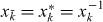 . For odd N, in addition to such pairs there is a single unpaired eigenvalue, denoted as xN, which (because of the constraint on the determinant) is pinned at xN = 1. The paired eigenvectors are related according to

Here we have to set ξk such that ξ2k = λk; this guarantees that the relation between both eigenvectors in a pair is reciprocal,  . Observing that the eigenvectors form an orthogonal basis, we find the matrix elements

With the help of these matrix elements we can now evaluate the drift and diffusion coefficients. In second-order perturbation theory,

where the prime restricts the sum to k ≠ l, while

is the increment of X to leading order in τ. The Gaussian averages are now carried out according to the rules


In particular,  ,
,  , and
, and
where we invoked equation (A.3). We thus obtain

Analogously, we find that

Note that these expressions only depend on the eigenvalues. We remark that for the pinned unpaired eigenvalue xN = 1, occurring if N is odd, these relations deliver  .
.
We now pass over to the quantities  , and restrict the index l such that it enumerates the pairs of eigenvalues. For even N we then find that

while for odd N we have

where the double prime excludes the pinned eigenvalue. Furthermore,

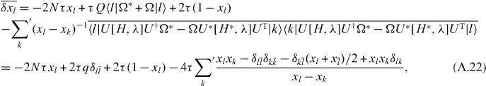
The stationarity condition of the associated Fokker–Planck equation (A.1) can be expressed as

For even N = 2M, this is solved by
up to a normalization constant. Each of the μn's (n = 1,2,...,M) is twofold degenerate. For odd N = 2M + 1 one eigenvalue is pinned at +1, and the remaining ones are twofold degenerate with the distribution

This concludes our derivation of the eigenvalue distribution of UU* with U uniform in  . We have not found the result (A.15) in the literature, but there is a curious correspondence with the known [36, 38] eigenvalue distribution of orthogonal matrices (uniformly distributed according to the Haar measure). An (N + 1) × (N + 1) orthogonal matrix O with determinant −1 has one eigenvalue pinned at −1. If we exclude that eigenvalue, the remaining N eigenvalues of O have the same probability distribution as the N eigenvalues of UU*.
A.3. Brownian motion of orthogonal matrices
As an independent demonstration of this correspondence between the eigenvalue distributions of UU* and O, we have investigated the Brownian motion of orthogonal matrices. Let O be a random (N + 1) × (N + 1)-dimensional matrix in the orthogonal group, constrained to the sector Det O = −1.
The Brownian motion is induced by O(1 + A + A2/2), where (in the fixed basis) A = −AT is a real antisymmetric matrix, with  . Due to the condition on the determinant, there is always one eigenvalue pinned at xN+1 = −1, while an additional eigenvalue is pinned at xN = 1 if N is odd. All other eigenvalues appear in pairs xl,
  , with
  (no additional factors are required).
We calculate the increments and average:


(Note that 〈l|A|l〉 does not vanish if |l〉 is complex, as is generally the case for the unpinned eigenvalues.)
As before, in passing to μl we restrict indices to enumerate different pairs. For N even, we find that (considering that the restricted sum has (N − 2)/2 terms)

while if N is odd (where the restricted sum has (N − 3)/2 terms),
Furthermore,

Comparison with equations (A.11)–(A.13) shows that these are the same average increments, if we rescale τ by a factor of 2. The eigenvalues of UU* and O therefore execute the same Brownian motion process, with the same stationary solution (A.15).
A.4. Symmetry class BDI
In class BDI, we have X = UλU†U*λUT, with U uniform in  and λ a fixed diagonal matrix with entries ±1 that sum up to Q. Since here the matrix X is symmetric, X = XT, it is now diagonalized by an orthogonal transformation; thus, the eigenvectors |k〉 = |k*〉 are real. As in class D, eigenvalues appear in complex-conjugate pairs, apart from eigenvalues pinned at 1. We observe that Ω mediates between the associated eigenvector,
 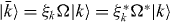 . In order to treat the partners symmetrically we have to require that
  is also real, so ξk compensates for any complex overall factor. It then follows that 〈k|ΩΩ*|k〉 = ξ2k = λk, and thus the coefficients ξk are related to the eigenvalues as in class D.
To identify the pinned eigenvalues note that Ω = Ω† = Ω−1 is both Hermitian and unitary, and thus has eigenvalues ±1. Let Ω± be the eigenspace for each set of eigenvalues, and Ω*± the analogous eigenspace for Ω*, which is spanned by the complex-conjugated vectors. We denote ξ = sign Q. The space [span(Ω−ξ,Ω*−ξ)]⊥ is then of dimension q = |Q| (barring accidental degeneracies), and all of the vectors in this space obey X|k〉 = |k〉. Thus X has q = |Q| eigenvalues pinned at 1. For each pinned eigenvalue, insisting that  implies Ω|k〉 = Ω*|k〉 = ξ|k〉, ξ = sign Q = ± 1 (consistent with the property that these states lie in the joint subspace of Ωξ and Ω*ξ).
With these additional properties in hand, the evaluation of drift and diffusion coefficients can proceed along the same steps as before. With the specified form of X, the incremental step of U carries over to an increment

where we have already averaged terms of second order in H; in particular, terms such as 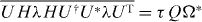 produce the topological invariant Q. The associated eigenvalue increment averages to
where the δlk term can be dropped because of the constraint k ≠ l on the sum. Note how Q changes to q = |Q| because of the sign of the matrix element involving pinned eigenvalues.
Again we find that eigenvalues at unity remain pinned. For the other eigenvalues, we separate out from the sum the q eigenvalues that are pinned, and sum over the M = (N − q)/2 pairs of unpinned eigenvalues,

where the double prime again indicates the exclusion of the pinned eigenvalues. Furthermore,

For the quantities  , this gives


The stationarity condition (A.14) is now fulfilled for

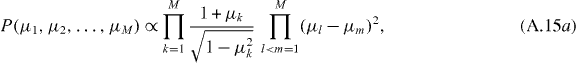
which gives the joint probability distribution of the twofold degenerate, unpinned eigenvalues μn (n = 1,2,...,M).
A.5. Eigenvalue density
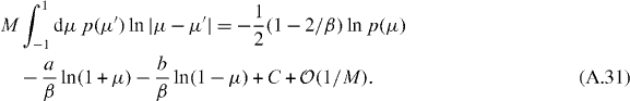
The probability distributions (A.15) and (A.27) are both of the form

with β = 2, a = 1/2, b = |Q| − 1/2 in class D and β = 1, a = 0, b = |Q|/2 − 1/2 in class BDI. These are called Jacobi distributions, because the eigenvalue density ρ(μ) can be written in terms of Jacobi polynomials [36].
For small N it is easier to calculate the eigenvalue density by integrating out all μn's except a single one. Keep in mind that |Q| of the μn's are pinned at unity and that the N − |Q| = 2M unpinned μn's are twofold degenerate. (The products in equation (A.28) run only over these M unpinned pairs.) The eigenvalue density 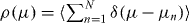 is then given by
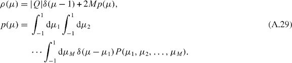
The delta functions satisfy 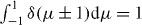 . The average conductance follows from the eigenvalue density according to equation (9),

This gives the small-N results in equation (11) and figure 2.
The large-N limit (14) is obtained from an integral equation for the eigenvalue density in the Jacobi ensemble [5, 39],
The constant C is determined by the normalization

The solution is


Upon substitution of the values for a,b,β into the two symmetry classes and transforming back from p to ρ, we find that

independent of Q and for both symmetry classes D and BDI. The corresponding result for the conductance is equation (14), to order 1/N if the limit N → ∞ is taken at a fixed Q.
A.6. Large-voltage limit
For completeness we also give the derivation of the large-voltage limit (10) of the average conductance. We need to evaluate

with  the density on the unit circle of the eigenvalues eiϕn of a unitary matrix
  .
.
In class D, the matrix  is uniformly distributed in
  . This is the circular unitary ensemble (CUE, β = 2). In class BDI, the chiral symmetry enforces that
  is unitary symmetric,
  with U uniform in
  . This is the circular orthogonal ensemble (COE, β = 1). Unlike the probability distributions we needed for the zero-voltage limit, these two distributions are in the literature [36],

The corresponding density

is uniform irrespective of the value of β and without any finite-N corrections. Substitution into equation (A.37) gives the result (10).
Footnotes
- 4
Two reviews of the search for Majorana fermions in superconductors are given in [8].
- 5
Chiral symmetry of the Hamiltonian is expressed by H↦ − H upon exchange
 of the electron and hole degrees of freedom. It is broken by spin–orbit coupling of transverse momentum, unlike the more fundamental particle–hole symmetry H↦ − H*.
 - 6
The Béri degeneracy of the Andreev reflection eigenvalues ρm ≠ 0,1 is a consequence of particle–hole symmetry, which is an anti-unitary symmetry that squares to +1. This distinguishes it from the more familiar Kramers degeneracy, resulting from an anti-unitary symmetry that squares to −1. For a self-contained proof of Béri degeneracy, see appendix B of [30].
- 7
- 8
The parameters for the simulations shown in figures 3 and 4 are, in panel (a): xbarrier = 23 lso, δLbarrier = 4a = 0.4 lso, Udisorder = 12.5 Eso, Ubarrier = 15 Eso, Gdisorder = 2.7 e2/h, Gbarrier = 1.8 e2/h; in panel (b): xbarrier = 3 lso, δLbarrier = a = 0.1 lso, Udisorder = 20 Eso, Ubarrier = 50 Eso, Gdisorder = 2.9 e2/h and Gbarrier = 3.2 e2/h.
- 9
- 10
- 11
The parameters for the simulations shown in figure 5 are: W = 0.3 lso, xbarrier = 2.7 lso, δLbarrier = a = 0.01 lso, EF = 1000 Eso, Δ0 = 100 Eso, Udisorder = 4000 Eso and Ubarrier = 7000 Eso, corresponding to N = 8, Gdisorder = 1.3 e2/h and Gbarrier = 1.5 e2/h.
- 12
The parameters for the simulations shown in figure 7 are: W = 0.3 lso, xbarrier = 1.1 lso, δLbarrier = a = 0.01 lso, EF = 200 Eso, Δ0 = 100 Eso, EZ = 60 Eso, Udisorder = 500 Eso and Ubarrier = 2000 Eso, corresponding to N = 2, Gdisorder = 1.5 e2/h and Gbarrier = 0.85 e2/h.