


Abstract
We study the infrared optical absorption properties of ABA- and ABC-stacked graphene multilayers using the effective mass approximation. We calculate the optical absorption spectrum at various carrier densities, and find the characteristic features that identify the stacking types and the number of layers. We fully include the band parameters and discuss detailed features such as trigonal warping and electron–hole asymmetry.
Export citation and abstract BibTeX RIS

Content from this work may be used under the terms of the Creative Commons Attribution 3.0 licence. Any further distribution of this work must maintain attribution to the author(s) and the title of the work, journal citation and DOI.
1. Introduction
In multilayer graphene systems, the weak interlayer coupling allows a variety of stacking structures, giving different electronic properties depending on the atomic configuration [1–10]. The most stable stacking arrangement between adjacent layers is known to be AB-stacking, where A sublattice on one honeycomb layer comes right below (or above) B sublattice on the other as illustrated in figure 1(b). In a graphene stack of more than three layers, there are two possible forms called ABA (hexagonal or Bernal) [11–16] and ABC (rhombohedral) stacking [17–19] as shown in figures 1(c) and (d), respectively. The ABA phase is the most stable and common, while some portion in natural graphite takes the ABC phase partly. The electronic band structure of multilayer graphene sensitively depends on the stacking arrangement. In AB-stacked bilayer graphene [20–24], the low-energy band dispersion becomes quadratic unlike the linear Dirac cone in a single layer [25–32]. In ABA-stacked multilayer, the spectrum consists of quadratic bands analogous to bilayer graphene and a linear band-like monolayer [26, 28, 29, 31–39], whereas the ABC multilayer has a completely different spectrum with a pair of flat low-energy bands at zero energy [26, 33, 35, 36, 40–46].

Figure 1. Lattice structures of (a) monolayer graphene, (b) AB-stacked bilayer graphene, (c) ABA-stacked multilayer graphene and (d) ABC-stacked multilayer graphene.
Download figure:
Standard imageTo investigate the electronic properties of layered graphene systems, optical measurement techniques are widely adopted. Raman spectroscopy is commonly used to determine the number of layers as well as the stacking structure [1, 4]. The angle-resolved photoemission spectroscopy is used to observe the electronic dispersion directly [21, 23]. Infrared spectroscopy is also widely applied to probe the low-energy band structure [47–58]. Theoretically, the optical absorption is related to the dynamical conductivity, and has been extensively studied for graphene and its multilayers [37, 38, 59–66]. The dependence of the infrared optical absorption on the stacking sequence has been observed in recent experiments [58] and also theoretically studied for graphene multilayers at neutral charge [66].
In this work, we study the dynamical conductivity of ABA and ABC graphene multilayers with various charge densities using the effective mass model. For each system, we calculate the spectral evolution as a function of charge density, and find several characteristic features that specify the stacking structure and the number of layers. We fully include possible band parameters and discuss the effect of additional features such as trigonal warping and electron–hole asymmetry. We study the graphene monolayer and AB-stacked bilayer in sections 2 and 3, respectively, and then consider the ABA and ABC multilayers (from three- to five-layer) in sections 4 and 5, respectively.
2. Monolayer graphene
Graphene is composed of a honeycomb network of carbon atoms as shown in figure 1(a), where a unit cell contains a pair of sublattices denoted by A and B. Electronic states in the vicinity of the K and K' points in the Brillouin zone are well described by the effective mass approximation [12, 13, 67–73]. Let |A〉 and |B〉 be the Bloch functions at the K point, corresponding to the A and B sublattices, respectively. In a basis (|A〉,|B〉), the Hamiltonian around the K point becomes

where p± = px ± ipy,  and v ≈ 1 × 10⁶ m s−1 is the band velocity [20, 74]. The velocity v is expressed as
  , where a = 0.246 nm is the lattice constant of the honeycomb lattice and γ0 = 3.16 eV is a band parameter that describes the electron hopping energy between the nearest A and B sites. The Hamiltonian at the K' point is obtained by exchanging p± in equation (1). The energy band is given by

with electron momentum p = (px,py) as quantum numbers and  . The carrier density at a given Fermi energy εF is given by

where gs = 2 and gv = 2 represent the degrees of freedom associated with spin and valley, respectively, and ns > 0 and ns < 0 represent electron concentration and hole concentration, respectively.
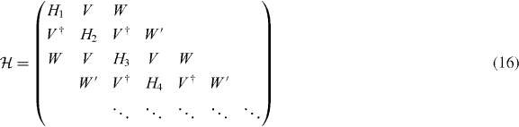
The optical absorption is related to the dynamical conductivity of the system. Within the linear response, the dynamical conductivity is generally given by

where S is the area of the system,  is the velocity operator, δ is the positive infinitesimal, f(ε) is the Fermi distribution function and |α〉 and εα describe the eigenstate and the eigenenergy of the system. In the following, we include the disorder effect by replacing δ with the phenomenological constant ℏ/τ ≡ 2Γ throughout the paper. The optical absorption intensity is related to the real part of σ(ω). The transmission of the light incident perpendicular to the two-dimensional system is given by [75]

For graphene, σ(ω) is written at zero temperature as [59]

where the first term in brackets represents the Drude (intra-band) part and the second the inter-band part. In the limit of Γ → 0, its real part goes to

where the Drude part becomes a delta function centered at ω = 0, and the inter-band part becomes a step function which is non-zero only when ℏω > 2|εF|, at the universal value,

The transmission of light incident perpendicular to the graphene sheet is then

showing that the absorption is given by πα ≈ 0.023 independent of frequency or wavelength, with the fine structure constant α ≡ e2/(cℏ) ≈ 1/137. This small absorption was experimentally observed [47–49], and is often used to identify the number of layers of graphene flakes created by mechanical exfoliation.
The real part of σ(ω) for several different charge densities ns is plotted in figure 2(b). The Hamiltonian of monolayer graphene is essentially scaleless, but to compare the multilayer's result in later sections, we set the unit of energy to γ1 ≈ 0.4 eV, and the unit of charge density to

where γ1 is the interlayer coupling in bulk graphite to be explained in the next section. The constant energy broadening is set to Γ = 0.01γ1 throughout the paper. We see the Drude peak at ω = 0 and the step increase of inter-band transition at ℏω = 2|εF|, as expected from equation (7).
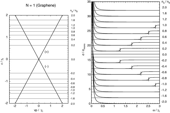
Figure 2. (Left) Band dispersion and (right) the real part of the dynamical conductivity as a function of frequency ω, of monolayer graphene with several different charge densities ns. The horizontal lines on the left indicate the Fermi energy corresponding to ns on the right. The vertical lines on the right attached to the curves indicate the energies at which the inter-band transition from s = −band to +band begins.
Download figure:
Standard imageIn a real system, the energy broadening Γ is not actually a constant but generally depends on the Fermi energy εF, and this becomes crucial when considering the static conductivity σ(ω = 0) at the Dirac point εF = 0. In the Boltzmann approximation, for example, [70] Γ is shown to be proportional to εF, so that the Drude part (the first term in equation (6)) at ω = 0 approaches a non-zero value in the limit of εF → 0, while it just vanishes at non-zero ω. Therefore, σ(ω;εF → 0) as a function of ω has a singularity at ω = 0 [59]. This anomaly remains even in more realistic calculations properly including the level broadening effects such as self-consistent Born approximation [70].
3. Bilayer graphene
Bilayer graphene [20–24] is a pair of graphene layers arranged in AB (Bernal) stacking as shown in figure 1(b). A unit cell includes A1 and B1 atoms on layer 1 and A2 and B2 on layer 2, and the layers are stacked with the interlayer spacing of d ≈ 0.334 nm, such that pairs of sites B1 and A2 lie directly above or below each other. There the interlayer coupling drastically changes the linear band structure of the monolayer, leaving a pair of quadratic energy bands touching at zero energy [25–32].
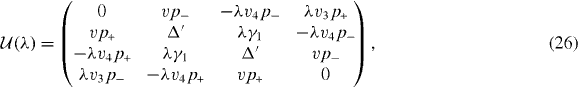
The effective mass Hamiltonian for bilayer graphene can be built using the Slonczewski–Weiss–McClure parameterization of tight-binding couplings of bulk graphite [11–16]. The parameter γ0 describes nearest-neighbor coupling between Ai and Bi within each layer, as already introduced for monolayer graphene. γ1 describes nearest-layer coupling between sites (B1 and A2) that lie directly above or below each other, γ3 describes nearest-layer coupling between sites A1 and B2 and γ4 is another nearest-layer coupling between A1 and A2, and between B1 and B2. The parameters γ2 and γ5 couple vertically located atoms on the next-nearest neighboring layers, and are thus absent in bilayer graphene. In ABA multilayer graphene illustrated in figure 1(c), γ5 connects a pair of atoms such as B1 and B3 belonging to the vertical column connected by γ1, whereas γ2 is for those which are not involved in the column, such as A1 and A3. We define Δ' as the energy difference between the sites which are in the γ1 column and the sites which are not. In the usual parameterization of the Slonczewski–Weiss–McClure model, we have Δ instead of Δ', and the two are related by Δ' = Δ − γ2 + γ5. For typical values of bulk graphite, we quote [16] γ1 = 0.39 eV, γ3 = 0.315 eV, γ4 = 0.044 eV, γ2 = −0.02 eV, γ5 = 0.04 eV and Δ' = 0.047 eV.
Using the above parameters, the effective Hamiltonian of bilayer graphene at the K point for the basis (|A1〉,|B1〉, |A2〉,|B2〉) is given by [25]
where v and p± are the same as for monolayer graphene, and v3 and v4 are defined as  and
and  . The effective Hamiltonian for K' can be obtained again by exchanging p+ and p−, giving the equivalent spectrum.
In the experimental situations, the top and the bottom layers may have different electrostatic potentials. This is particularly important when the charge carriers are doped by the gate electrode, which induces a perpendicular electric field at the same time. The interlayer potential difference generally modifies the band structure of the multilayer graphene system [25, 26, 28–30, 46, 76, 77] and affects the optical absorption spectrum [56, 78]. The effect of the gate-induced band distortion on the optical spectrum was investigated for the bilayer graphene [78]. Here, for simplicity, we neglect the interlayer potential difference even in the doped case, while such a situation can be actually realized in an experimental setup using both the top and bottom gate electrodes [79].
When the parameters v3, v4 and Δ' are switched off in equation (11), the eigenenergies become [25, 26]

The branch μ = − gives a pair of conduction (s = +) and valence (s = −) bands touching at zero energy. The other branch μ = + is another pair repelled away by ±γ1. In the following, we use the notation μ = 2,1 instead of +,− and specify the four energy bands as (s,μ) = (±,1),(±,2). In ε ≪ γ1, the subbands (±,1) touching at zero energy are approximately expressed as a quadratic form

In this model (equation (12)), the inter-band part of the dynamical conductivity is explicitly written as [38, 62]
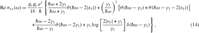
where we assumed that |εF| < γ1. The first three terms in brackets are the absorptions from the valence band to the conduction band, where the first term is from the band (−,1) to (+,1), the second from (∓,1) to (±,2) and the third from (−,2) to (+,2). The fourth term is present only in electron- or hole-doped cases, and is caused by a transition between the two conduction bands (+,1) and (+,2) or between the valence bands (−,1) and (−,2). It is expressed by a delta function in ω because in the present approximation (equation (12)), the bands (±,1) and (±,2) have identical dispersion except for an energy shift by γ1.
When the parameters v3, v4 and Δ' are included, the low-energy band equation (13) is modified to [44]

where tan φ = py/px and ξ = ± is the valley index (K and K'). The parameter v3 produces trigonal warping where the energy band around each valley is stretched in 120° symmetry [25]. The tiny parameter v4 gives the common quadratic term to both the conduction and valence bands, and thus breaks the electron–hole asymmetry. The parameter Δ' appears in the second order of Δ'/γ1 in equation (15) and is neglected there, while it gives a positive energy shift Δ' to both (±,2). As a result, the energy distance between (+,1) and (+,2) bands becomes larger than between (−,1) and (−,2).
Figures 3(a) and (b) are the band structure and Re σxx(ω) calculated for the bilayer graphene of equation (11) with the band parameters fully included. The curve for the non-doped case ns = 0 has essentially no prominent structure except for step-like increases near ℏω = γ1, corresponding to transitions from (−,1) to (+,2) and from (−,2) to (+,1). The energy difference between the two transitions is due to the electron–hole asymmetry introduced by Δ'. When εF is shifted from the charge neutral point, a strong peak appears near ℏω = γ1 given by the transition from (±,1) to (±,2) with ± for electron and hole doping regions, respectively. The peak corresponds to the delta function in equation (14), but it is now broadened because the trigonal warping caused by γ3 distorts the lower energy bands (±,1) more seriously than (±,2), so that the transition energy depends on k. We also observe a step-like feature at ℏω ∼ 2εF such as monolayer graphene's, which corresponds to the first term in equation (14).
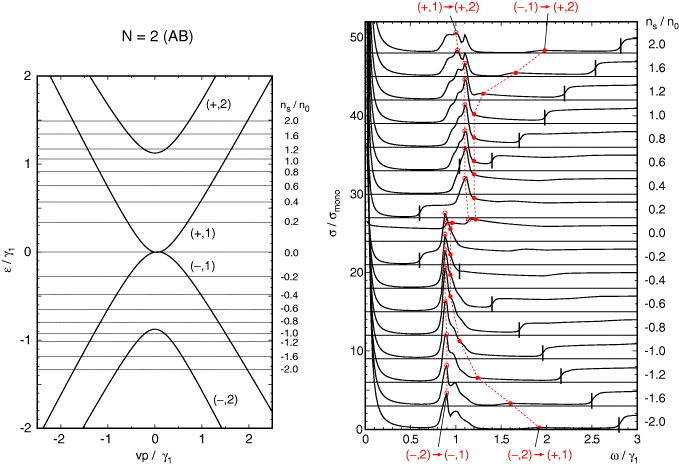
Figure 3. (Left) Band dispersion and (right) the real part of the dynamical conductivity as a function of frequency ω, of bilayer graphene. On the right, the symbols connected by dotted lines indicate the peak energies of some inter-band transitions. The vertical lines indicate the energies at which the transition from the highest hole band (−,1) to the lowest electron band (+,1) begins.
Download figure:
Standard image4. ABA-stacked multilayer graphene
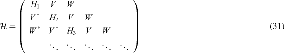
The calculation of dynamical conductivity can be extended to graphene multilayers with more than two layers in a straightforward manner. Here we consider an ABA-stacked graphene multilayer composed of N layers illustrated in figure 1(c), which contains Aj and Bj atoms on the layer j = 1,...,N. In ABA stacking, the sites B1,A2,B3,A4,... are arranged along vertical columns normal to the layer plane, while the rest of the sites A1,B2,A3,B4,... are above or below the center of hexagons in the neighboring layers. If the bases are sorted as |A1〉,|B1〉; |A2〉,|B2〉; ...; |AN〉,|BN〉, the Hamiltonian around the K point becomes [26, 28, 29, 31, 32, 34, 38]
with
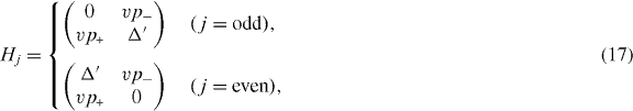

with the band parameters already introduced in the previous section. The diagonal blocks Hj describe intralayer coupling in layer j, V nearest-neighbor interlayer coupling and W and W' next-nearest-neighbor interlayer coupling. The effective Hamiltonian for K' is obtained by exchanging p+ and p−.
The Hamiltonian can be approximately decomposed into subsystems equivalent to monolayer or bilayer graphene [34, 37, 38, 80]. The dynamical conductivity of the system can then be written as a summation over each sub-Hamiltonian, so that the absorption spectrum becomes essentially equivalent to the collection of the effective monolayer and bilayer's spectra [37, 38]. The decomposed subsystems are labeled by index m, which is defined as

The subsystem m is composed of four bases um = {|ϕm(A,odd)〉,|ϕm(B,odd)〉,|ϕm(A,even)〉,|ϕm(B,even)〉} with

where X is A or B, and


and


Obviously, fm(j) is zero on even j layers, while gm(j) is zero on odd j layers. A superscript such as (A, odd) indicates that the wave function has a non-zero amplitude only on |Aj〉 sites with odd j.
The Hamiltonian matrix between um and um' becomes [38, 80]

where
and


 , appearing in diagonal blocks (m = m'), is equivalent to the Hamiltonian of bilayer graphene with nearest-layer coupling parameters multiplied by λm.
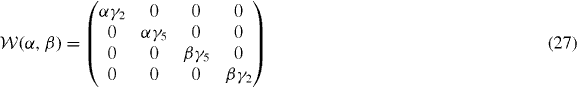
  with m = m' adds on-site asymmetric potential to this effective bilayer system
  . For a pair of low-energy bands near zero energy, it causes an overall energy shift of (α + β)γ2/2 and an energy gap of ∼|(α − β)γ2| at the band touching point, as in asymmetric bilayer graphene.
The case of m = 0 is special in that gm(j) is identically zero, so that only two basis states {|ϕ(A,odd)0〉, |ϕ(B,odd)0〉} survive in equation (20). The matrix for the m = 0 block for the two remaining bases is

which, barring the diagonal terms, is equivalent to the Hamiltonian of monolayer graphene. Therefore, odd-layered graphene with N = 2M + 1 is composed of one monolayer-type and M bilayer-type subsystems, while even-layered graphene with N = 2M is composed of M bilayers but no monolayer. The subsystems with different m's are not exactly independent but mixed by off-diagonal matrix elements W with m ≠ m', which contains only the next-nearest interlayer couplings, γ2 and γ5. This is responsible for small band repulsion at crossing points between different m's, while the overall band structure is well described by only retaining the diagonal blocks [38].
The trilayer graphene N = 3 has a monolayer block (m = 0) and a bilayer block (m = 2) with  . The band structure is shown in figure 4(a), where the symbols M and B represent the monolayer and the bilayer block. The dynamical conductivity for several ns's is plotted in figure 4(b). This actually looks like a summation of monolayer in figure 2 and bilayer in figure 3, while the prominent peak of the bilayer block shifts from ℏω ∼ γ1 to λ2γ1. Also, the peak is broader than the real bilayer graphene in figure 3, because the trigonal warping effect is more pronounced for larger λm [34].
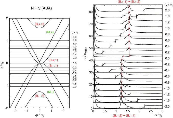
Figure 4. A plot similar to figure 3 for ABA three-layer graphene.
Download figure:
Standard imageFigures 5 and 6 show similar plots for N = 4 and 5, respectively. The band structure of four-layer graphene is composed of a bilayer-like band with a wide splitting (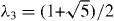 , indicated as 'B') and another bilayer-like band with a narrow splitting (
 , 'b'). As a result, the spectrum is composed of a broader peak at ℏω ∼ λ3γ1, and a narrower peak at λ1γ1. The same is true for five-layer graphene which contains two bilayer blocks
  ('B') and λ2 = 1 ('b') and one monolayer block ('M').
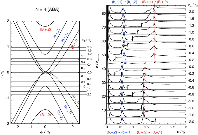
Figure 5. A plot similar to figure 3 for ABA four-layer graphene.
Download figure:
Standard image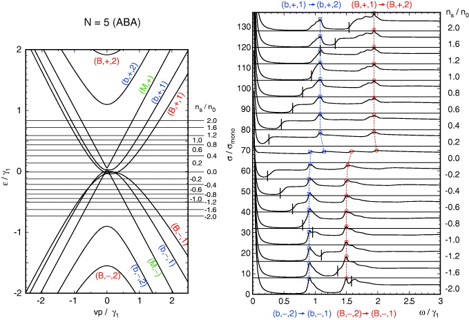
Figure 6. A plot similar to figure 3 for ABA five-layer graphene.
Download figure:
Standard image5. ABC-stacked multilayer graphene
The electronic structure of the ABC-stacked multilayer is quite different from ABA and so is the optical absorption spectrum. In the ABC lattice structure, Bi and Ai+1 are always vertically located as illustrated in figure 1(d). In the bases |A1〉,|B1〉; |A2〉,|B2〉; ... ; |AN〉,|BN〉, the Hamiltonian around the K point becomes [19, 26, 40, 46]

The effective Hamiltonian for K' is again obtained by exchanging p+ and p−.
The overall band structure can be understood by considering the simplest model only including v and γ1. The system is then regarded as a one-dimensional chain depicted in the side panel of figure 1(d), in which Aj and Bj are coupled by vp± and Bj and Aj+1 by γ1 [26]. At p = 0, the connections between Aj and Bj are lost so that the eigenstate set is composed of (N − 1)-fold degenerate dimer states between Bj and Aj+1 at each of ε = ± γ1, and two-fold degenerate states localized on A1 and BN at zero energy. When infinitesimal p is switched on, the dimer states are coupled by a term linear to p giving a set of (N − 1) linear bands at each of ε = ± γ1, whereas zero-energy states at A1 and BN are coupled by Nth-order perturbation in p, leading to weak dispersion (vp)N/γN−11 [26, 36, 42, 44]. We number the mth conduction band and valence band from the center as (+,m) and (−,m) (m = 1,2,...,N), respectively. The bands with m = 1 correspond to the nearly zero-energy bands and m = 2,...,N to the dimer-state bands at ±γ1. The band structures of ABC multilayers N = 3,4,5 with all the band parameters included are presented in the left panels of figures 7–9, respectively. The effects of the additional parameters are similar to those in bilayer graphene. γ3 and γ2 cause trigonal warping of the band dispersion [44] and γ5 and Δ' cause a shift in the dimer-state bands at ±γ1 toward the upper energy.
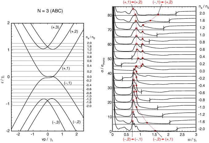
Figure 7. A plot similar to figure 3 for ABC three-layer graphene.
Download figure:
Standard image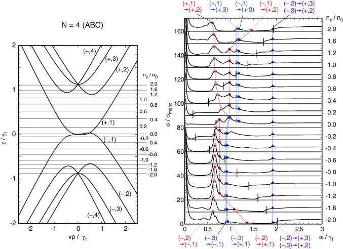
Figure 8. A plot similar to figure 3 for ABC four-layer graphene.
Download figure:
Standard image
Figure 9. A plot similar to figure 3 for ABC five-layer graphene.
Download figure:
Standard imageThe absorption spectra of ABC multilayers shown in the right panels of figures 7–9 are obviously different from their ABA counterparts. At N = 3, the spectrum for the doped system is characterized by a strong peak due to the transition between (±,1) and (±,2) similar to bilayer graphene, whereas the peak center is significantly smaller than ℏω = γ1. This is because the band energy of (+,2) decreases when p shifts from zero, so that the distance between (+,1) and (+,2) tends to be smaller than the value at p = 0, which is about γ1. We also note that the peak of the transition between (∓,1) and (±,2) is much more pronounced here than in bilayer, owing to the large density of states of the flat surface state bands near p = 0. The transitions related to the highest band (±,3) are almost invisible, because the band dispersion is conical and contributes to only a small density of states. In ABC multilayers with N = 4 and 5, the peak of the transition between (±,1) and (±,2) moves even lower ω as N increases, reflecting deeper band bottom of (±,2) with respect to ±γ1. We also see that the transitions involving (±,3) become gradually observable, as the band bottom of (±,3) becomes flatter with increasing N.
6. Conclusion
We calculated the optical absorption spectra of graphene multilayers with ABA and ABC stackings with several different thicknesses. We traced the spectral evolution with varying charge density, and observed the characteristic features that may be useful in identifying the stacking sequences as well as the number of layers. We found that the absorption spectrum of ABA multilayer is characterized by strong peaks corresponding to the transitions within the decomposed bilayer subband, and they can appear in a wide frequency region, 0 < ℏω < 2γ1. In ABC multilayers, on the other hand, the main peaks are given by the transition from the zero-energy surface state band to the excited bands near ±γ1, and the main peak energies are always around γ1 or lower. Here we neglect the interlayer potential asymmetry given by the gate electric field, while it is expected to cause broadening and shift of the absorption peaks via the band deformation, as observed in the bilayer graphene [56, 78]. Detailed investigation of those effects for ABA and ABC multilayers is left for future works.
Acknowledgment
This work was funded by the JST–EPSRC Japan–UK Cooperative Programme under grant no. EP/H025804/1 and by Grants-in-Aid for Scientific Research No. 24740193 from JSPS.