


Abstract
Nitrogen–vacancy centers in diamond have outstanding quantum optical properties that enable applications in information processing and sensing. As with most solid-state systems for quantum photonic applications, the great promise lies in the capability to embed them in an on-chip optical network. Here we present basic integrated devices composed of diamond micro-ring resonators coupled to waveguides that are terminated with grating out-couplers. Strong enhancement is observed for the zero-phonon line of nitrogen–vacancy centers coupled to the ring resonance. The zero-phonon line is efficiently coupled from the ring into the waveguide and then scattered out of plane by the grating out-couplers.
Export citation and abstract BibTeX RIS

Content from this work may be used under the terms of the Creative Commons Attribution 3.0 licence. Any further distribution of this work must maintain attribution to the author(s) and the title of the work, journal citation and DOI.
GENERAL SCIENTIFIC SUMMARY Introduction and background. The nitrogen–vacancy (NV) center in diamond is a point defect in which one carbon atom has been replaced by a nitrogen atom, and a neighboring carbon atom is missing. The NV center has quantum states with long-lived coherence, and these states can be easily controlled using optical and microwave fields. These properties are expected to enable applications in information processing and sensing. As with other optically addressable solid-state systems, the great promise of NV centers for quantum applications lies in the capability to embed them in a large-scale on-chip optical network. This could allow entanglement to be produced across a large collection of quantum systems on the same chip.
Main results. We demonstrate a prototype on-chip optical network made from mono-crystalline diamond on a silicon dioxide substrate. The device consists of a micro-ring optical resonator coupled to a diamond waveguide. When the optical transitions between the quantum levels of a NV center are in resonance with the micro-ring, light emitted from the NV center can be efficiently channeled into the waveguide, which in the future will connect to a larger on-chip optical network.
Wider implications. The device reported in this manuscript is a first step towards a large-scale on-chip network. Future work will focus on demonstrating optical control of NV centers embedded in photonic networks, and devices where multiple NV centers are interconnected. The devices described in this work could eventually enable large-scale quantum networks with applications in quantum simulation, chemistry, communications and factoring.
1. Introduction
During the last decade, diamond has become an intensely researched optical material for quantum photonic devices [1]. The main reason behind this development is that diamond can serve as a host material for a variety of color centers with desirable quantum optical properties. Of all these color centers, the negatively charged nitrogen–vacancy (NV) center has attracted the most attention because of its long spin coherence time and an energy-level structure that allows for straightforward optical initialization and readout of the quantum states [2, 3]. Current applications for NV centers in diamond include magnetic and electric field sensors with ultra-high spatial resolution, and devices for quantum information [4–7]. For quantum information applications, a possible path toward scalability is to connect a set of NV centers using an on-chip optical network [8]. We have previously demonstrated proof-of-concept devices where single NV centers are coupled to micro/nano resonators in single-crystal diamond [9, 10]. Here we take the next step toward the development of optical quantum networks and demonstrate that the zero-phonon emission from NV centers located in ring resonators is enhanced and then efficiently coupled to photonic ridge waveguides and scattered out of the plane of the chip. A similar approach has been shown in [11], but here we demonstrate operation at cryogenic temperatures and thus resonant enhancement of the zero-phonon line (ZPL) as required for quantum information applications.
2. Device fabrication
The device used in this experiment consists of a diamond micro-ring (4.5 μm in diameter and 500 nm wide) coupled to a ridge waveguide (300 nm wide). The spacing between the ring and the waveguide is ≈100 nm (figure 1). The grating output coupler consists of alternating diamond slabs (350 nm wide) separated by 200 nm (we would like to specify that this design does not provide optimal coupling efficiency, and we give the details of a better design toward the end of this paper). The entire device was etched in a ≈300 nm thick diamond membrane that was obtained by thinning a 5 μm thick type IIa single-crystal diamond membrane (purchased already polished to 5 μm from Element 6) using reactive ion etching (RIE) in an oxygen plasma. During the etching process outlined in figure 2 the membrane was mounted on a 2 μm thick SiO2 substrate thermally grown on an Si wafer. After the membrane preparation, the device was patterned using electron-beam lithography and negative electron-beam resist (HSQ, Fox-12), which further acted as a mask to transfer the pattern into diamond using RIE with oxygen/argon plasma (see figure 2 for details). Some residual resist remained on the top of the diamond after etching.

Figure 1. View of the device consisting of a micro-ring resonator coupled to a ridge waveguide. The waveguide is terminated with two grating couplers used to couple light into and from the waveguide. (The images are not of the actual device used in the experiment because imaging with a scanning electron microscope can change the charge state of the NV center. A similar device was imaged instead.)
Download figure:
Standard image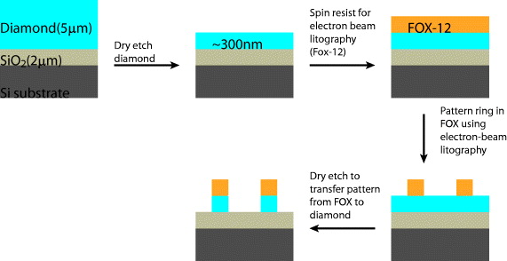
Figure 2. Schematic representation (not to scale) showing the sequence of fabrication steps. A 5 μm-thick diamond membrane was placed on a 2 μm-thick thermal SiO2 layer grown on a silicon wafer. No special mounting procedure was used to attach the membrane to the substrate. The fabrication steps were as follows. (i) Dry etching (oxygen plasma in an Oxford RIE etching machine) was used to thin the membrane until it was ≈300 nm thick. (ii) Electron-beam resist (Fox 12) was spun on the chip and electron-beam lithography was used to pattern the ring in the resist. (iii) The pattern was transferred from resist to the diamond using dry etching in oxygen plasma.
Download figure:
Standard image3. Passive measurements of the cavity–waveguide coupling
The optical properties of the device were first characterized via a transmission measurement, where a laser beam was coupled into one of the gratings and the intensity of the light scattered from the other grating was monitored as shown schematically in figure 3(a). The input coupling and the collection were done using the same confocal microscope setup. The output light was separated from the direct reflection of the laser by re-imaging the chip with a lens and using a movable aperture located in the image plane to select only the area of interest (i.e. the grating) from the chip. The output was sent to a photodetector, which in this case was the CCD of a spectrometer that was later used to measure the signal from NV centers coupled to the resonator.

Figure 3. (a) Schematic representation showing the principle of the transmission measurement, where a laser is injected in one of the gratings and the intensity of the light scattered from the other port is monitored as a function of wavelength. (b) Transmission scan through a ring resonance. The fit indicates a coupled quality factor Qcoupled = 5500 and a contrast close to 90%.
Download figure:
Standard imageThe results of this measurement are shown in figure 3(b) where a continuous wave laser diode (NewFocus Velocity) was scanned across a ring resonance that was later coupled to the spectral line of an NV center. A fit to the data indicates a coupled quality factor of Qcoupled = 5500 and a contrast of 90%. A similar ring uncoupled to the waveguide had a quality factor of Quncoupled = 12 000, which indicates that the device operates close to the critical-coupling regime (Qcoupled = Quncoupled/2) where 100% contrast is expected.
4. Low-temperature spectroscopy of nitrogen–vacancy centers
To estimate the coupling of the NV ZPL emission to the mode of the ring resonator and then into the waveguide, the sample was cooled in a continuous-flow liquid helium cryostat, at temperatures below 10 K. The same confocal setup used for the transmission measurement was utilized. A green laser (532 nm) was used to excite photoluminescence (PL) in NV centers as shown in figure 4(a), and an NV center with resonance frequency close (red-shifted) to the ring resonance frequency was identified. A gas condensation technique was then used to tune the ring resonance until it overlapped with the NV spectral line as described in our previous work [9]. As in [9], the NV center exhibits strong spontaneous emission rate enhancement that is observed as a large increase in the scattered PL in the ZPL.
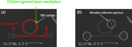
Figure 4. (a) Schematic representation showing the principle of the PL measurement. An NV center located in the diamond ring and optically coupled to it is excited with green (532 nm) laser light (6 mW). The NV center emits red light (≈637 nm) that first circulates in the ring; then it is coupled to the waveguide and scattered outward by the gratings. (b) A movable aperture is used to collect light that is scattered only from specific areas of the device, as indicated by the dashed-line circle.
Download figure:
Standard imageTo quantify how much of the ZPL luminescence is actually coupled into the waveguide, we used a movable aperture in the re-imaged plane of the device (the same configuration as for the transmission measurement) to collect light from different areas of the device and send it to a spectrometer. The relative size of the aperture compared to the device and the locations of interest are shown in figure 4(b). The spectra taken when the NV was resonant with the cavity are shown in figure 5, both when an aperture was used to collect only light scattered by the right grating and also when no aperture was used. This indicates that most of the PL collected in the microscope objective comes through the right grating (the left grating for this device was not scattering the light efficiently due to errors in the fabrication process). In figure 5, we also show a comparison between the spectrum taken with the aperture on the right grating when the NV was on resonance, and when the cavity was detuned from the NV. This indicates that having the cavity resonant with the NV is essential for obtaining high count rates into the waveguide. The two effects responsible for increasing the count rate are the higher coupling efficiency into the waveguide, and the spontaneous emission rate enhancement (Purcell effect). For a ring that is critically coupled to the waveguide, the waveguide coupling efficiency is 50%.
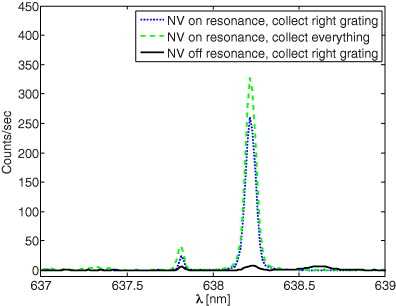
Figure 5. Comparison between the PL collected with the aperture over the right grating when the NV is resonant with the cavity (blue dot), PL collected without an aperture from the entire device (green dash) and PL collected with the aperture from the right grating when the cavity is off-resonant with the NV (black line).
Download figure:
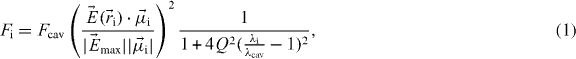
Standard imageThe spontaneous emission rate enhancement of a particular dipole transition i of an emitter coupled to a micro-resonator relative to the rate of that dipole in an infinite uniform medium of the same material as the resonator is enhanced [12] by the factor  . The rate 1/τ0 is the emission rate in the uniform dielectric medium, 1/τleak is the emission rate outside the cavity mode and
where  is the dipole moment,
  is the local electric field at the emitter location
  , λcav is the cavity wavelength, λi is the emitter wavelength and
  is the maximum value of the electric field in the resonator. For the case where the dipole is resonant with the cavity and also ideally positioned and oriented with respect to the local electric field, Fi = Fcav, where

and  is the optical mode volume of the resonator, with
  the electric permittivity at position
  . The mode volume of the resonance coupled to the NV center is
  and the quality factor is Qcoupled ≈ 5500, which corresponds to a maximum spontaneous emission rate enhancement Fmax ≈ 29. Our measurements indicate a spontaneous emission rate enhancement F ≈ 12, as determined from lifetime measurements similar to those presented in our previous work where a similar spontaneous emission rate enhancement was estimated [9]. With a waveguide coupling efficiency of 50% and a spontaneous emission rate enhancement of F ≈ 12, it is expected that ≈6 times more ZPL photons are coupled into the waveguide than all the photons emitted by a single NV in bulk material. In figure 6, the ZPL collected from the right grating is compared to the ZPL collected from NVs located in a region of bulk (i.e. un-patterned) membrane. Integrating over the entire spectral width of the NV for both the coupled and un-coupled cases, we determine that in the coupled case we collect ≈25 times more photons scattered from only one of the gratings than what we can collect from bulk NV centers using a microscope objective with NA = 0.6 and free-space optics.

Figure 6. Comparison between the PL collected from the right grating when the NV and the cavity are resonant (blue) and the PL collected from NVs located in an un-patterned region of the membrane (yellow).
Download figure:
Standard imageTo improve the out-coupling efficiency from the waveguide through the grating and into the free space optics, it is essential to improve the design for the grating out couplers. Here we present a design (see figure 7) for a grating that scatters out of plane the transverse magnetic (TM) mode in the waveguide, and ∼40% of the scattered light can be collected by a microscope objective with numerical aperture NA = 0.6. The design consists of a grating where the grooves have different widths as shown in figures 7(a) and (b). As light travels through the grating it gets scattered and thus diminishes in intensity. The light first interacts with grooves of smaller width and then the width is increased such that the amount of scattered light at each groove has similar intensity and constructively interferes in the out of plane direction. The entire structure is designed in a 300 nm thick diamond membrane situated on top of a silicon dioxide layer. The grooves of the grating are situated at locations [0,0.2784,0.5761,0.8930,1.2292,1.5847] μm (the location of the origin is arbitrary) and have widths [0.0623,0.0783,0.0958,0.1148,0.1353,0.1574] μm. The tapered region is 7 μm long and the waveguide width is 2 μm at the location of the grating. The profile of the electric field density when the waveguide is excited with a TM source is shown in figures 7(c) and (d) (the simulation is performed using a finite difference time domain simulation). It can be observed that the light is scattered primarily in the out of plane directions in a narrow solid angle. The amount of energy scattered into NA = 0.6 was determined by analyzing in k-space the field profile on top of the structure.
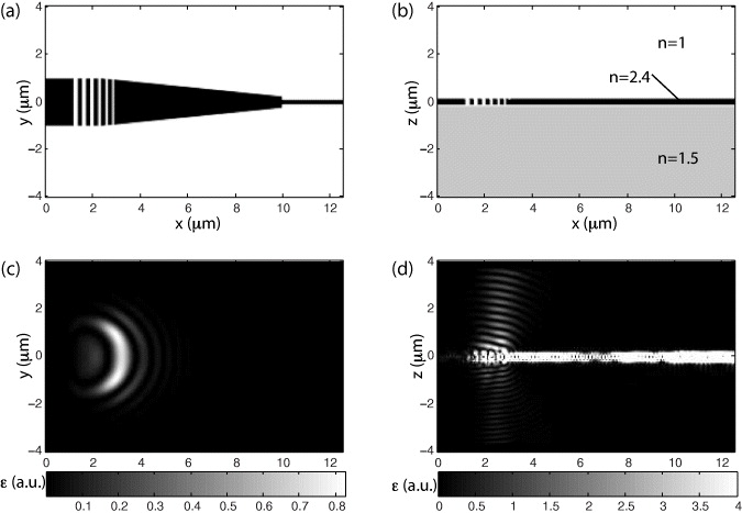
Figure 7. (a) Top view of the grating structure connected to the waveguide via a tapered waveguide. The black region corresponds to a high refractive index (diamond). The units on the axes are microns. (b) Cross section through the grating along the waveguide. The diamond grating (n = 2.4) sits on top of a silicon dioxide layer (n = 1.5), while the top material is air. (c) Electric field density in a plane located 2.5 μm above the grating. (d) Electric field density (ε) in a plane perpendicular to the plane of the grating and going through the waveguide.
Download figure:
Standard image5. Conclusion
In conclusion, we have demonstrated efficient coupling of the ZPL PL of NV centers in diamond into on-chip photonic waveguides and used grating couplers to scatter a portion of this light into free space optics. This represents an initial step toward the implementation of on-chip photonic networks in diamond. Future work will focus on developing devices based on multiple NV centers including on-chip interference of the ZPL from at least two NVs that is a prerequisite for implementing on chip entanglement of multiple NV centers. Entanglement between multiple NVs on the same chip could eventually enable large-scale devices such as quantum simulators, with applications in quantum chemistry [13], quantum communications and factoring [14].
Acknowledgment
This material is based upon work supported by the Defense Advanced Research Projects Agency under award no. HR0011-09-1-0006 and The Regents of the University of California.