


Abstract
We demonstrate for the first time the ability to perform time resolved imaging of terahertz (THz) waves propagating within a photonic crystal (PhC) slab. For photonic lattices with different orientations and symmetries, we used the electro-optic effect to record the full spatiotemporal evolution of THz fields across a broad spectral range spanning the photonic band gap. In addition to revealing real-space behavior, the data let us directly map the band diagrams of the PhCs. The data, which are in good agreement with theoretical calculations, display a rich set of effects including photonic band gaps, eigenmodes and leaky modes.

Content from this work may be used under the terms of the Creative Commons Attribution 3.0 licence. Any further distribution of this work must maintain attribution to the author(s) and the title of the work, journal citation and DOI.
1. Introduction
The field of terahertz (THz) polaritonics, in which THz-frequency electromagnetic radiation is controlled in a ferroelectric crystalline slab, has seen major advances in THz generation, control, and detection in the past decade [1]. Using femtosecond optical pulses, THz radiation can be generated directly in the ferroelectric crystals lithium niobate (LiNbO3) or lithium tantalate (LiTaO3) through impulsive stimulated Raman scattering [2]. Waveguiding of the THz field in the ferroelectric slab allows for direct detection and manipulation of fields over long (typically mm) distances. Control over THz generation is accomplished by spatiotemporally shaping the optical driving pulses [3, 4], and subsequent wave propagation can be influenced by integrated photonic elements [5–7]. Furthermore, it is possible to characterize the interactions of the THz fields with these elements via time-resolved, phase-sensitive imaging [8] and to display the images from separate measurements in 'movie' form that shows wave propagation at light-like speeds through the material.
During this same time period, photonic crystals (PhCs) have emerged as versatile tools for controlling radiation across the electromagnetic spectrum [9]. Their ability to manipulate light comes from their unique dispersion relations and the presence of the photonic band gap (i.e. a range of frequencies for which light cannot propagate inside the PhC [10, 11]). Bulk PhCs and PhCs embedded in slab waveguides (PhC slabs) have been used to fabricate structures which can guide [12, 13], filter [14–17], and enhance fields in small volumes and PhC defect sites [18–20]. In order to characterize these systems, measurements have typically involved analyzing far-field reflected or transmitted signals (e.g. [12, 15, 21–23]). More recently near-field scanning optical microscopy studies have probed the near-fields close to the surfaces of PhC structures [17, 24–28]. However, these are unable to measure electric fields (E-fields) directly and are only sensitive to the evanescent fields outside the PhC structures. Furthermore, it has been shown that the tips used in these near-field experiments can couple to the evanescent fields [20] and may perturb the measurements. Because of these experimental limitations, understanding of PhC behavior has come primarily through simulations [29–32] along with far-field measurements. These considerations highlight the need for an experimental method that can directly measure the near-fields inside the PhC to verify theoretical predictions and investigate the effects of imperfect structures and unique material properties. The polaritonics platform can meet this need for PhC slabs, where such insights are especially useful because this compact slab geometry is more easily realized in existing device architecture than the 2D PhC analog that is effectively infinite in the third dimension.
In this work we use the THz polaritonics platform to directly observe near-fields in PhC slabs and to evaluate the extent to which simulations corroborate the experimental findings. We had two main motivations for developing PhC slabs in the polaritonics platform: first, to advance the polaritonics platform by adding the versatile control capabilities of PhCs, and second, to improve general understanding of PhCs, in particular in the PhC slab geometry, by directly recording the spatiotemporal evolution of waves within the crystal. Various photonic components have been designed based on PhCs across the electromagnetic spectrum. Integrating these structures onto the polaritonics platform creates new possibilities for manipulating THz fields (e.g. routing and filtering THz fields directly on the polaritonics chip) and could easily be combined with the capabilities to arbitrarily shape THz fields. PhCs also enhance the possibility of using the polaritonics platform for executing electro-optic and potentially all-optical circuits through the use of active materials in the structural elements. The platform naturally lends itself to the fabrication of PhC slabs because the high dielectric contrast between the host materials ( eo
≈ 26 for LiNbO3 and eo
≈ 38 for LiTaO3 at THz frequencies [1]) and air results in extremely efficient scattering at the interfaces. PhC slabs have been fabricated on the polaritonics system in the past [33, 34], but it was not possible to measure the fields inside the PhC because of insufficient imaging capabilities and sample preparation techniques. Recently, improved imaging methods [8] have enabled direct observation of the fields within densely machined structures such as the PhCs. In addition, a newly developed hydrofluoric acid (HF)-assisted laser machining process [35] is capable of cutting holes into ferroelectric slabs while maintaining the surface optical quality necessary for optical imaging methods (see figure 1(a)).
eo
≈ 26 for LiNbO3 and eo
≈ 38 for LiTaO3 at THz frequencies [1]) and air results in extremely efficient scattering at the interfaces. PhC slabs have been fabricated on the polaritonics system in the past [33, 34], but it was not possible to measure the fields inside the PhC because of insufficient imaging capabilities and sample preparation techniques. Recently, improved imaging methods [8] have enabled direct observation of the fields within densely machined structures such as the PhCs. In addition, a newly developed hydrofluoric acid (HF)-assisted laser machining process [35] is capable of cutting holes into ferroelectric slabs while maintaining the surface optical quality necessary for optical imaging methods (see figure 1(a)).
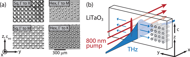
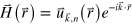
Figure 1. (a) Optical microscope images of the square (Sq) and hexagonal (Hex) PhC lattices studied. The air holes were cut by ultrafast laser machining. The orientation of the optic axis (c-axis) relative to the primitive lattice vectors is given in the lower left. For all measurements, the THz field propagated in the y-direction. (b) Experimental geometry. The 800 nm pump pulse passes through the LiTaO3 slab, launching counterpropagating THz waves which are polarized along z and waveguided in the y-direction away from the generation region. The field shown schematically is the lowest order TE mode of the unstructured slab.
Download figure:
Standard image High-resolution imageStudying wave propagation in PhCs with the polaritonics platform has four major advantages over other methods. First, the electro-optic detection that is used is exclusively sensitive to the fields inside the host material. Second, the femtosecond optical pulses used in imaging of THz waves provide deeply subwavelength spatial and subcycle temporal resolution [8]. Furthermore, since the imaging fully captures the E-field of the waves within the crystal, rather than just the envelope of the field, the amplitude and phase of the waves can be analyzed directly. Finally, the detection is non-perturbative because there is no tip or other element introduced in the near-field and the weak probe light does not significantly influence the THz fields [36, 37]. We studied THz-frequency PhC slab structures in classic geometries that have been embedded in a LiTaO3 host, which is relatively isotropic compared to LiNbO3 (|eo
− o
| ≈ 4 for LiTaO3 compared to 15 for LiNbO3 [1]). We measured the spatiotemporal evolution of the fields within PhCs and characterized the behavior of waves with frequencies within the photonic band gap, generated dispersion (or band) diagrams for the PhC slabs, and compared our experimental results to calculated band diagrams. We observe bound modes, leaky modes, and waves whose frequencies lie within the band gap. While our present work focuses on well-known PhC geometries and behaviors, our ability to image and characterize the near-fields within PhCs is only now possible because of recently developed imaging and machining capabilities. These can be used in the future to observe more interesting wave phenomena (e.g. negative refraction). As new theoretical ideas for PhC devices are developed, direct visualization of the E-fields will be a valuable tool for testing and verification.
2. Theory of PhCs
Here we present concepts of PhCs that are useful for our analysis. These topics have been discussed in many different texts, for example in [9] or [38]. PhCs are a special class of mixed dielectric materials in which the different constituents are periodically arranged. Bloch's theorem says that the solutions to Maxwell's equations for the magnetic field (H-field) can be written because is periodic (i.e. ). Here is an envelope function with the same periodicity as which can be expanded as a Fourier series


are the reciprocal lattice vectors defined such that where N is an integer, ensuring the periodicity of . The envelope function, then, is a sum of plane waves with successive wave vectors that differ by a reciprocal lattice vector. A further consequence of Bloch's theorem is that only solutions in the first Brillouin zone (BZ) are unique [9]. The full set of solutions is found by solving the eigenvalue problem given below:


where ωn is the wave vector-dependent eigenfrequency. The band structure for the PhC is obtained by determining the set of eigenfrequencies for given values of propagation wave vector k. Various numerical methods exist for computing the band diagrams of 2D and 3D PhC structures (e.g. see appendix D of [9]). In this work, the simulated band structures of PhC slabs were calculated using a freely available plane wave eigensolver package [39].
In PhCs, the presence of symmetry elements (e.g. mirror planes, rotation axes) allows the eigenmodes to be classified by how they transform with respect to these symmetry operations. In PhC slabs specifically, there is a mirror plane bisecting the thin dimension of the slab (the x-axis in figure 1(b)), and the modes are categorized depending on whether the field profile is even or odd with respect to the mirror plane. Modes with even symmetry are often referred to as TE-like modes, while modes with odd symmetry are TM-like modes [9].
The final consideration we have for these PhCs is on the different kinds modes. Here, the full set of modes that can propagate are the eigenmodes described by equation (1), as well as leaky modes. In a lossless material, eigenmodes are guided infinitely within the PhC and propagate without attenuation because they are bound by total internal reflection. In contrast, leaky modes have a finite lifetime [40, 41] and decay in amplitude as they propagate. Leaky modes exist when a PhC is fabricated in a slab waveguide when a mode can transfer power into the surrounding environment, air in this case [31]. These electromagnetic waves can be described qualitatively as

This qualitative behavior is similar to that of waves with a frequency within the band gap of the PhC, or evanescent waves [9]. Unlike evanescent waves, however, leaky waves are able to transfer power into the surrounding medium.
3. Experimental
The experiments were performed using an amplified ultrafast Ti:Sapphire system (800 nm center wavelength, 100 fs duration, 1 kHz repetition rate, 1.5 mJ pulse energy). Holes were cut clear through the x-cut 54 μm thick LiTaO3 slabs using a homebuilt, femtosecond laser machining system. A protective layer of SiO2 was deposited on both sides of the slab prior to machining. After machining, the SiO2 and LiTaO3 debris ejected by the machining process were removed by an HF etch, revealing the optical-quality sample surface [35]. The minimum feature size was ∼3 μm and the bevel around each hole was ∼2 μm. A square lattice or a hexagonal lattice of air holes was cut into the host LiTaO3 with a lattice constant of 100 μm (see figure 1(a)). The radius of the holes was 35 μm for the square lattice and 25 μm for the hexagonal lattice. The holes had a slightly square shape rather than perfectly rounded circles due to slight imperfections in the laser machining setup. In order to measure the thickness and dielectric constant for simulations, we recorded the dispersion curves for TE waves polarized along the extraordinary axis in an unstructured region of the slab [42]. The resulting curves were fit to analytical solutions for the dispersion curves of a plain dielectric slab waveguide. Slab thickness and dielectric constant were the only fitting parameters. The LiTaO3 slab thickness was 54 ± 1 μm. We found eo
= 41.45 ± 0.02. o
= 41.6 ± 0.7 was obtained by measuring multiple etalon reflections of a THz wave propagating along the x-axis. Simulations were performed using these values.
The laser power was divided 90:10 for the pump and probe arms, respectively. The pump pulse was directed to a retroreflector on a mechanical delay stage and focused to a line parallel to the optic axis (c-axis) of the LiTaO3 slab (the z-axis in the figures) using a cylindrical lens, launching vertically extended, z-polarized counterpropagating THz waves. The refractive index at THz frequencies is far higher than at the 800 nm pump wavelength, and the THz waves that in a bulk crystal would propagate in directions given by a Cherenkov angle [43, 44] are waveguided within the slab as shown schematically in figure 1(b). The polarization of the pump beam was parallel to the c-axis of the crystal ensuring maximal THz generation efficiency by taking advantage of the largest electro-optic coefficient (r33) [44].
The probe pulse (100 fs duration, 200 nJ pulse energy) was the output from a home-built non-collinear optical parametric amplifier tuned to 532 nm. The probe was expanded to illuminate a large portion of the sample, thereby setting the experimental field of view. As the THz wave travels through the LiTaO3 slab, it changes the crystal's refractive index via the electro-optic effect. As a result, the expanded probe beam develops a spatially dependent phase shift directly proportional to the THz E-field. This phase shift must be converted to a change in amplitude so it can be detected directly on a camera. We accomplish this by imaging the sample with a self-compensating polarization gating imaging system [8]. In addition to phase-to-amplitude conversion, this method keeps all the fabricated structures and the THz field itself in focus and suppresses noise through balanced imaging. Noise was further suppressed by implementing lock-in imaging at a detection frequency of 500 Hz using a high-speed CMOS camera and an optical chopper in the pump beam. By moving the mechanical stage, the time delay between the arrival of the pump and probe is changed and the full spatiotemporal evolution of the THz field can be recorded as a sequence of images that can be played back as a movie.
4. Results
4.1. Visualizing waves in PhC
We recorded images of THz TE-waveguide modes interacting with the structure. The THz waves were generated in a non-machined portion of the slab and propagated toward a square array of air holes machined into the LiTaO3 host with a lattice constant of 100 μm (see figure 1(b)). Figure 2(a) shows a series of images (assembled into the online supplementary movie 1) and figure 2(b) shows a magnified view of the fields within the lattice. The images shown are generated by dividing the signal frame (THz pulse present) by the reference frame (THz pulse absent). The two counterpropagating waves, shown 5 ps after THz generation by the pump pulse, are travelling away from the generation region, which is visible as a faint gray line midway between the waves. When the rightward-moving wave reaches the PhC, some of the frequencies are strongly reflected, indicating the presence of a photonic band gap. The waves that enter the PhC couple to both TE-like and TM-like modes and continue to propagate through the structure. We can also clearly see evidence of dispersion as different frequency components propagate at different speeds. The THz waves in the PhC also travel at a different velocity compared to the unstructured slab [33], further demonstrating different dispersion relations.

Figure 2. (a) A series of images from the online supplementary movie 1 showing THz wave propagation through a square PhC with a lattice constant of 100 μm. The air holes are false-colored black for clarity. The black arrows at the top indicate the wave propagation directions, revealing the wave reflected by the PhC starting at 10 ps. (b) Close-up view of the THz near field inside the PhC. (c) A space–time plot generated by averaging over the vertical dimension of the frames in movie 1. The PhC structure begins at 0 mm. (d) The result of a Fourier transform along the time axis of the portion of (c) enclosed by the dashed white lines. (e) A line-out from (d) showing the amplitude at 0.47 THz (red dashed) and an exponential decay fit to the maxima of the signals between holes (blue).
Download figure:
Standard image High-resolution imageAlthough the movie contains all the spatial and temporal information about the waveform, a more compact representation of the data is a space-time plot in which the x-axis of the space-time plot is the lateral propagation distance and the y-axis is the time delay between the pump and probe. Since the generated THz fields are essentially uniform along the vertical dimension (z-axis in figure 1(b)) the spatial profile of the wave at each time delay can be calculated by averaging over this dimension [42]. This results in a 1D row vector from each frame of the movie, and repeating the process for the frame at each time delay generates a 2D matrix or the space–time plot seen in figure 2(c). Here, the optical pump pulse located at a position of −0.3 mm arrives at the sample at t = 0, launching two THz waves that move in opposite directions in the LiTaO3. When the rightward-propagating wave encounters the edge of the PhC lattice at 0 mm, some of the wave is reflected while the rest continues into the PhC. The positions in the space–time plot where the signal is smaller (vertical gray bars cutting through the wave) occur because of the air holes. Since the THz waves can only be detected in LiTaO3, averaging over the air holes reduces the signal at those positions. Photonic band gaps can be determined from space–frequency plots like the one shown in figure 2(d), which are calculated by Fourier transforming the space–time plot in figure 2(c) along the time axis. As observed in figure 2(d), frequencies within the photonic band gap (between 0.36 ± 0.02 and 0.54 ± 0.01 THz) are reflected efficiently and only penetrate a short distance into the PhC.
Theory predicts that inside the PhC, waves within the band gap are evanescent, described by complex propagation wave vectors k = k' + iγ, and their amplitudes decay exponentially due to coherent reflections [9]. This was verified experimentally in figure 2(e) which shows a line-out of the amplitude at ∼0.47 THz. By fitting the amplitude of the field inside the PhC to the function A * exp(−y/Y), a decay constant of Y = 90 ± 3 μm is extracted. A simulation of the fields at that frequency radiating from a line defect (a line of holes with radius 15 μm instead of 35 μm) within the structure gives a decay length of 71 μm. Waves within the first band gap in this geometry have wavelength λ = 2a = 200 μm. This means that the wave does not complete a full oscillation period or penetrate one unit cell before the field decays to 1/e of the initial value. The short decay length is due to the high index contrast between LiTaO3 and air.
4.2. Determination of eigenmodes and leaky modes
In order to map out the dispersion diagram, the pump beam was focused directly onto the laser machined region such that THz waves were generated inside the structured portion of the slab. This generated both TE-like and TM-like modes and allowed us to analyze rightward and leftward propagating waves at the same time. Figure 3(a) shows the data represented in a space–time plot. A 2D Fourier transform converts space and time axes into wave vector and frequency axes, respectively, which generates the dispersion diagram [42] shown in figure 3(b) for ω ⩾ 0. The different BZs are between the dashed black lines located at k = (π + 2πn)/a where n is an integer. The regions with positive and negative frequency correspond to the waves moving to the left and right, respectively, in the space–time plot. The mirror symmetry with respect to k = 0 indicates that the dispersion is the same regardless of the direction of wave propagation.

Figure 3. (a) Space–time plot of THz waves generated directly inside a square PhC. The edges of the image are the edges of the photonic crystal. (b) Dispersion diagram obtained from a 2D Fourier transform of the space–time plot in (a). The region highlighted in yellow represents the light cone. The regions highlighted in orange show the locations of the leaky modes. (c) A section of the experimental dispersion diagram in (b) with the dispersion curve of the lowest-order mode for a homogeneous dielectric slab waveguide overlaid. The thickness used in the calculation was 54 μm and the dielectric constant was 25.
Download figure:
Standard image High-resolution imageThe observed signals repeat every k = 63 rad mm−1, consistent with the size of BZ for the square lattice in this orientation. The amplitude of the signal in the different BZs indicates the magnitude of the corresponding Fourier series coefficient used to describe the PhC modes (see equation (1)). This particular distribution can be understood by considering the set of holes as a perturbation of the unstructured slab. In this case we expect that the eigenmodes of the resulting PhC should be similar to the slab waveguide modes, with modulations due to the periodic structure. Figure 3(c) illustrates this by plotting the dispersion curve of an unstructured, homogeneous slab on top of the experimental dispersion diagram. The homogeneous dispersion curve was calculated using a dielectric constant of 25, which is close to the volume-weighted average of the dielectric constants of LiTaO3 and air in the PhC unit cell. Based on the calculated curve, we expect the lowest mode to have the largest amplitude in the first BZ, while the higher order modes have larger amplitudes in the second or third BZs. Even though the full bandwidth of possibly generated frequencies spans 0.1 to 1.5 THz, the evanescent waves are not bound within the PhC slab and scatter rapidly into free space, evident by the weak amplitude in these spectral regions in figure 3(b).
The signals that are observed in the measured dispersion diagram correspond to both eigenmodes and leaky modes of the PhC. The faint orange triangles in figure 3(b) indicate the locations of the leaky modes and the faint yellow triangle in figure 3(b) indicates the light cone [31]. As stated in section 2, leaky modes differ from eigenmodes in that leaky modes are able to couple to the external radiation, thereby transferring energy out of the slab. The coupling occurs because waves can change momentum by scattering off the lattice, whereby their wave vectors change by an integer multiple of the reciprocal lattice vector. Thus any wave with its frequency within the light cone and with a wave vector separated from the light cone by a multiple of the reciprocal lattice vector is 'leaky,' and will eventually scatter away. Leaky modes can be uniquely identified in angle-resolved measurements [45] and have been engineered to enhance the coupling of fluorescent emission for single emitters [46], to improve the extraction efficiency from LEDs [47, 48], and to enhance nonlinear interactions [49]. Because the leaky modes decay slowly compared to the subcycle time resolution of our measurement, they are strong features in the experimental dispersion diagrams in figure 3(b). Direct observation of leaky modes in the medium in which they propagate has been reported for acoustic modes [50] and in some cases for electromagnetic modes [40]. The present experimental platform provides a facile means for leaky mode observation. In addition, control over the generation of leaky modes through experimental selection of the THz wave vector and frequency is possible through the use of spatially and temporally tailored excitation light fields [3, 4].
4.3. Mapping out dispersion curves and comparison with theory
In a PhC, dispersion depends strongly on the relative angle between the principal lattice vectors of the periodic structure and the direction of wave propagation because the structures lack continuous rotational symmetry. In order to vary the relative angle while keeping the THz polarization along the LiTaO3 c-axis (z-axis of the crystal, see figure 1) and thereby keeping the same THz generation and detection efficiency [21, 42], we machined PhCs in different orientations in the LiTaO3 slab (see figure 1(a)). This allowed us to measure dispersion along the paths that directly connect the high-symmetry points of reciprocal space (see figure 4). A square lattice was machined with the primitive lattice vectors oriented such that the THz wave vectors were between the Γ point and the X point (along the dashed green line) in the square lattice reciprocal space (see figures 1(a) and 4(a)). By rotating the primitive lattice vectors 45°, the wave vectors also were rotated so that they lay between the Γ point and the M point (along the dashed blue line) instead of the X point. Two hexagonal lattices were fabricated (see figures 1(a) and 4(c)), one such that the THz wave vectors were between Γ and M and the other with the crystal rotated 90° so the wave vectors ranged from the Γ point through the K point and finally to the M point in an adjacent BZ.

Figure 4. Reciprocal space map and dispersion diagram for the square lattice (a), (b) and the hexagonal lattice (c), (d). For the square lattice, the lattice spacing is a = 100 μm and the hole radius is r = 35 μm. For the hexagonal lattice, a = 100 μm and r = 25 μm. For the square lattice a rotation of 45° switches the THz propagation vector between Γ–X and Γ–M. For the hexagonal lattice a rotation of 90° switches the THz propagation vector between Γ–M and Γ–K–M. In (a), (c) the first BZ is indicated in orange. In (b), (d) analytical solutions of eigenmodes (solid red lines) and leaky modes (dashed orange lines) with the appropriate symmetry are overlaid on top of the data.
Download figure:
Standard image High-resolution image
Figure 4 shows the reciprocal space maps and band diagrams of the two PhC lattices in different orientations. The reciprocal space maps in figures 4(a) and (c) are centered around the first BZ and repeat themselves in the k1 and k2 directions. In the dispersion diagrams in figures 4(b) and (d), repeated signals were observed and so we only show half of the first and second BZs. For all the structures, we observed a subset of both the TE-like and TM-like modes, dictated in part by the overlap between the excitation field 'line' profile and the spatial patterns of the modes. The numerically solved band diagrams are overlaid on the experimental data. Solid red lines represent eigenmodes and dashed orange lines correspond to leaky modes. We observe good agreement between experiment and theory for the generated modes, indicating that the deviation of the holes from being perfectly circular does not appear to have a large effect on the bands within the structure.
Information on the band gaps for the different PhC geometries is summarized in table 1. The sizes of the band gaps are expressed as the ratios of the gap widths to their center frequencies, which are unbiased measures of band gap size [9]. The band gaps observed are comparable to those resulting from earlier structures fabricated in LiNbO3 for IR (hexagonal lattice, gap size ∼38%) [18] and THz (hexagonal lattice, gap size ∼14%) [33] wavelengths, gallium arsenide at IR wavelengths (hexagonal lattice, gap size ∼18%) [41], and aluminum gallium arsenide at NIR (hexagonal lattice, gap size ∼30%) [15, 31]. The large variation in the size of square PhC band gaps suggests that the structure could be used as a variable frequency filter by simply rotating the crystal. In contrast, the fact that the hexagonal lattice band gap is relatively insensitive to orientation means that it can be effectively used as an omnidirectional mirror for TE modes.
Table 1. Band gap information for PhC geometries.
| Lattice type | Symmetry point | Band gap size (%) | Center frequency (THz) |
|---|---|---|---|
| Square | X | 40 | 0.45 |
| Square | M | 11 | 0.50 |
| Hexagonal | K | 24 | 0.46 |
| Hexagonal | M | 29 | 0.44 |
As mentioned before, some of the generated bands were TE-like while others were TM-like. There are many additional modes of both polarizations (not shown in our calculated results) that lie within the generation bandwidth, but only those with the correct symmetry and polarization can be excited in this geometry [41, 51]. As a result the band gaps observed in these measurements are 'incomplete' band gaps. This is an important consideration when designing devices based on the PhC architecture, where the function of the device depends not only on the spectral location and size of the band gap, but also on which modes are propagating within the crystal. While the location of the band gap can be determined by far-field measurements, direct measurement of the PhC dispersion through near-field observation provides additional information (e.g. which modes including leaky modes are excited within the PhC slab and with what efficiencies, and how far each mode propagates) that can be useful for a wide range of near-field applications, for example those in which a defect such as a missing hole within the structure is used as a resonator or similar device and the full position and time-dependent field in the region is of interest.
5. Conclusions
We observed the time-resolved propagation of THz waves directly within a PhC slab. From the full spatiotemporal evolution of the waves, we were able to determine the dispersion curves along different reciprocal lattice vector directions. We observed several important classes of PhC behavior, including band gaps, eigenmodes, and leaky modes. The complete spatiotemporal and spectral characterization of waves including the near-fields within patterned regions enables detailed comparison to PhC theory. Our data were in good agreement with theoretically predicted band structures. Our method is sensitive not only to the eigenmodes of the system, but also to leaky modes that are often difficult to observe directly and are sometimes neglected in theoretical descriptions of PhCs. While our measurements were focused on PhC slabs at THz frequencies, the scale invariance of Maxwell's equations means that the insights gained here are applicable to PhCs that operate at any part of the electromagnetic spectrum. Thus the polaritonics system is an excellent general testbed for PhC devices. In present measurements, the near-fields within aperiodic structures are under investigation. Although here we have focused on static properties, electro-optic and acousto-optic properties of LiNbO3 and LiTaO3 or optical excitation of material introduced into the air holes of our present structures could enable actively controllable devices that could be used for high speed optical modulation and signal processing.
Acknowledgments
This work was supported by the National Science Foundation under grant no. 1128632. BKO was supported in part by an NSF GRFP fellowship and PS was supported by a Canadian Research Fellowship. We thank Prof Steven Johnson and Mr Chia Wei Hsu for help with simulations and for helpful discussions.