


Abstract
The temperature-dependent Coulomb screening and excitation spectrum of electrons in silicene are studied by the tight-binding model and the random-phase approximation. With the spin–orbit interaction, monolayer silicene is a narrow-gap semiconductor. At finite temperatures, the interplay between the intraband and interband transitions could lead to an undamped plasmon mode at low frequencies. The plasmon mode only exists in a limited region of temperature and momentum, corresponding to the constrained gap transition. Beyond that region, another damped plasmon mode dominates the excitation spectrum. The drastic change in the plasmon behavior might be observed experimentally, which could allow for the identification of the spin–orbit energy gap.
Export citation and abstract BibTeX RIS

Content from this work may be used under the terms of the Creative Commons Attribution 3.0 licence. Any further distribution of this work must maintain attribution to the author(s) and the title of the work, journal citation and DOI.
1. Introduction
A carbon nanosheet, namely graphene, was discovered a few years ago. Its unique linear bands at low energy provide scientists with an abundance of new physics, including the Klein paradox for tunneling through a potential barrier [1–3], the anomalous quantum Hall effect [4, 5], and the peculiar optical properties [6–10]. After the successes in graphene, scientists intensified their search for other graphene-like two-dimensional (2D) materials [11–13]. In the most recent years, silicene, a nanosheet composed of silicon atoms, has been synthesized [14–16]. In the same group of the periodic table with graphene, silicene is predicted to exhibit similar electronic properties. Besides, it could be better than graphene for two main reasons. The first is its compatibility with current Si-based device technologies. The second is its sizable energy gap (Eg), owing to the larger magnitude of the atomic spin–orbit interaction (SOI) and the buckling structure. The buckling structure means that the two sublattices sit at different planes in the vertical direction, which mainly results from the larger ionic size of silicon atoms. Other group-IV crystals, e.g., Ge and Sn, are also expected to appear in this form for their 2D structures [17, 18]. The significant SOI is predicted to bring about many interesting physics, such as the spin Hall effect [19–21] and the optically-generated spin-valley-polarized charge carriers [22–25].
The collective Coulomb excitations, dominated by the e–e interactions, are important to understand the behavior of electrons in a material. Many studies have investigated the essential properties in graphene systems [26–33]. However, so far in silicene the relevant studies are still limited [34–36] and do not take into account the temperature effects. In an intrinsic monolayer graphene, low-frequency plasmons hardly exist, mainly due to the vanishing density of states at the Fermi level. It requires a thermal population of electrons (holes) in the conduction (valence) band to induce the intraband plasmon, which is a weakly damped mode [26]. This is explained by the strong dependence of the carrier density on temperature, as a result of the semi-metallic property. A similar feature may appear in monolayer silicene. However, the largest difference could be the constrained low interband transitions out of the spin–orbit energy gap. In this article, we provide the results, calculated by the tight-binding model and the random-phase approximation, of the Coulomb excitation spectra of monolayer silicene with and without SOI. The former condition suggests an undamped plasmon mode induced at nonzero temperatures ( ). The plasmon main features are decided by the ratio of intraband to interband excitations. In other words, they are tunable by varying the momentum transfer (q) and the temperature. A transformation from the undamped plasmon to another damped one is observed during the change in q and T. Therefore, two different plasmon modes exist, arising from different theoretical mechanisms; this is clarified in the corresponding dielectric functions. The critical q and T to cause the significant damping rate in the plasmon excitation could be measured by experiments. Either critical value might be useful to determine the strength of the spin–orbit coupling.
2. Methods
Similar to graphene, silicene consists of a honeycomb lattice of silicon atoms with two sublattices made up of A and B sites. The difference is that it has a buckled structure with the two sublattice planes separated by a distance l = 0.23  . In the tight-binding approximation, the Hamiltonian for silicene in the presence of SOI is written as [18, 37]

where  (
( ) creates (annihilates) an electron with spin polarization α (β) at site i (j). The sum is taken over all pairs of nearest neighbor
  or next-nearest-neighbor
  lattice sites. The first term in equation (1) is the usual nearest-neighbor hopping with the transfer energy t = 1.6 eV. The second term describes the effective SO coupling with
  = 3.9 meV.
  is the vector of Pauli matrices. vij is determine by the orientation of the two nearest bonds connecting the next-nearest neighbors, i.e.
  = +1 (−1) if the next-nearest-neighboring hopping is anticlockwise (clockwise) with respect to the positive z axis. The third term is the intrinsic Rashba SO coupling with
  meV, where
  with
with  connects two sites i and j in the same sublattice, and
  means the A(B) site. The tight-binding Hamiltonian can also be used to describe other group-IV elements, such as germanium with a different set of parameters t = 1.3 eV,
  = 43 meV,
  = 10.7 meV, and l = 0.33
  [18].
[18].
When the system is perturbed by a time-dependent Coulomb potential, the electron–electron interactions would induce a charge density fluctuation which acts to screen the external perturbation. This dielectric screening determines the normal modes of the charge density oscillations. Electronic excitations are characterized by the transferred momentum q and the excitation frequency ω, which determine the dielectric function. The dynamical dielectric function, calculated within the random-phase approximation, is

where  is the in-plane Fourier transformation of the bare Coulomb potential energy, and
  = 2.4 is the background dielectric constant due to the deep-energy electronic states [38]. The linear response function is given by [38, 39]
The Fermi–Dirac distribution is ![$f(E)=1/\{1+{\rm exp} [(E-\mu )/{{k}_{{\rm B}}}T]\}$](https://content.cld.iop.org/journals/1367-2630/16/12/125002/revision1/njp504968ieqn19.gif) , where kB is the Boltzmann constant. μ is the chemical potential and is set to zero over the range of the symmetric conduction (c) and valence (v) bands under the investigation. Γ is the energy broadening which results from various de-excitation mechanisms.
, where kB is the Boltzmann constant. μ is the chemical potential and is set to zero over the range of the symmetric conduction (c) and valence (v) bands under the investigation. Γ is the energy broadening which results from various de-excitation mechanisms.
3. Results and discussion
The unscreened excitation spectrum, related to single-particle excitations (SPEs), is studied firstly. Without SOI, monolayer silicene, similar to graphene, exhibits linear bands at low energy (the black curve in the inset of figure 1(b)). At T = 0, the interband excitations are the only excitation channel. The threshold excitation energy is expressed as  =
=  (
( 105 m s−1). This makes the real part of dielectric function
  and the imaginary part
  divergent in the forms of
  and
and  [40], respectively, shown by the black curves in figures 1(a) and (b) for q = 1 in unit of
  . With SOI, a band gap is opened between the conduction and valence bands with the creation of the 2D band-edge states (the red curve in the inset of figure 1(b)). Correspondingly,
  is shifted to a higher frequency around
  , shown by the red curves in figures 1(a) and (b). Meanwhile, the square-root divergent structures in
  and
and  are changed into a step-like and a logarithm-divergent form, respectively. This is more evident for a smaller q. The step-like structure in
  represents the occurrence of the inter band-edge-state transitions.
  is connected with
  by the Kramers–Kronig relations and remains positive over the entire frequency region with or without SOI. This means that no prominent plasmon excitations could survive at zero temperature.

Figure 1. The dielectric functions as a function of ω at T = 0 ((a) and (b)), T = 50 K ((c) and (d)), and T = 100 K ((e) and (f)) for q = 1.  (left panels) and
  (right panels) represent the real and the imaginary parts, respectively. The energy bands are plotted in the inset of (b). The red and black curves show the condition with and without SOI, respectively. The energy broadening width
  meV. q is in unit of
  .
.
Download figure:
Standard image High-resolution imageAt finite temperatures, intraband transitions are allowed, which changes the special structures of  drastically. For q = 1 and T = 50 K, without SOI, the intraband transitions predominate the excitation properties (black curves in figures 1(c) and (d)).
  and
and  exhibit an asymmetric dip and peak at
  , respectively. Here,
  corresponds to either the highest intraband or the lowest interband excitation energy.
  has two zero points, associated with a weakly damped plasmon mode of the system located where
  is relatively small. Compared with the SPEs at T = 0, the decreased
  at
at  is responsible for the weakening of the interband correlation, as a result of the occupation of electrons (holes) in the conduction (valence) band. In the presence of SOI (red curves in figures 1(c) and (d)), a peak associated with the band-gap transition emerges in
  with the frequency higher than that of the dip. For monolayer graphene, the two structures may merge due to the relatively weak SOI. Corresponding to the separation of the
  peak from its dip, an excitation gap is developed in
  . One of the
  zero points is located in the
  gap, where an undamped plasmon mode occurs. When
  is over the energy gap, the gap transition becomes negligible gradually. In that case, the
  zero point moves to a higher frequency where
  is finite (figures 1(e) and (f)), i.e., the plasmon turns into a damped mode. Meanwhile, the influence of SOI on the dielectric functions becomes smaller, known from the comparison between the black and red curves.
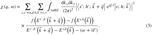
In order to better understand the condition that allows a long lived plasmon,  density plots of
  are displayed in figures 2(a) and (b). At T = 0 (figure 2(a)), the interband SPEs exist above
  (the dashed curve). Below
  is a SPE-forbidden zone. At a finite temperature, i.e. T = 50 K (figure 2(b)), the intraband SPEs are induced below
  (the low dashed curve). There is a SPE gap between the interband (the up dashed curve) and the intraband boundaries. In that region the appearance of a long lived plasmon (an undamped mode) is possible. This requires the coexistence of intraband and interband-gap transitions, as discussed in figures 1(c) and (d). The coexistence of the two SPE channels at q = 1 mainly happens in the range: 25 K
  100 K, as illustrated in figure 2(c) for the
  density plot of
  . For
. For  K, more electrons occupy at where the state energies are larger than the interband-gap-excitation energy. Then, the intraband transitions begin to dominate the SPE spectrum.
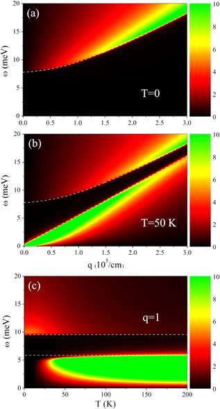
Figure 2.
 density plots of
  at (a) T = 0 and (b) T = 50 K. The
  density plot of
  is shown in (c) for q = 1. The white dashed curves in each panel indicate the SPE boundaries. The color scale stands for the intensity of
  .
.
Download figure:
Standard image High-resolution imageThe energy-loss function (∝ ![${\rm Im}[-1/\epsilon ]$](https://content.cld.iop.org/journals/1367-2630/16/12/125002/revision1/njp504968ieqn69.gif) ), related to the screened excitation spectrum, is used to understand the collective-excitation mode of electrons. Each prominent structure in
), related to the screened excitation spectrum, is used to understand the collective-excitation mode of electrons. Each prominent structure in ![${\rm Im}[-1/\epsilon ]$](https://content.cld.iop.org/journals/1367-2630/16/12/125002/revision1/njp504968ieqn70.gif) may be considered a plasmon excitation with different degrees of Landau damping. For monolayer silicene,
may be considered a plasmon excitation with different degrees of Landau damping. For monolayer silicene, ![${\rm Im}[-1/\epsilon ]$](https://content.cld.iop.org/journals/1367-2630/16/12/125002/revision1/njp504968ieqn71.gif) at T = 0 exhibits a plateau at low frequency (the insets in figures 3(a) and (b)), meaning that the charge excitation is mainly single-particle like. This is similar to bilayer graphene, in which a plasmon mode dominated by the interband SPEs is also obscure due to the strong Landau damping [29, 41]. When the temperature is higher than a critical value (
at T = 0 exhibits a plateau at low frequency (the insets in figures 3(a) and (b)), meaning that the charge excitation is mainly single-particle like. This is similar to bilayer graphene, in which a plasmon mode dominated by the interband SPEs is also obscure due to the strong Landau damping [29, 41]. When the temperature is higher than a critical value ( K for q = 1), a prominent peak is induced either without SOI (figure 3(a)) or with SOI (figure 3(b)). The peak with SOI is featured by the lower frequency, the stronger intensity, and the narrower spectral width than that without SOI as a result of the weakened Landau damping. Besides, the plasmon peak in the two conditions (with and without SOI) exhibits the different dependence on the temperature and momentum. When T grows, there are more free carriers. In the case of SOI = 0, this increases the peak intensity and frequency monotonically (similar to the result in monolayer graphene [26]). However, with SOI, the peak intensity is first enhanced and then suppressed. Therefore, an abrupt change in the plasmon behavior is observed at a critical temperature, as discussed later in figure 5. On the other hand, the plasmon peak for SOI = 0 is suppressed with the increment of q (figure 3(c)), owning to the decreased number of intraband-excitation channels. While, for
  (figure 3(d)), the plasmon peak is first enhanced and then weakened with the increasing q, which reflects the competition relation between the intraband and the gap transitions.

Figure 3. The energy-loss functions are plotted in (a) and (b) for various  at q = 1. Those for different
  at T = 100 K are shown in (c) and (d). (a) and (c) for SOI = 0, and (b) and (d) for
  . The condition of T = 0 is plotted in the insets of (a) and (b).
Download figure:
Standard image High-resolution imageThe q-dependent behavior of the low-frequency plasmons is important in understanding their characteristics. Figures 4(a)–(c) show the results for various  . The lower (upper) dashed curve in each figure represents the maximum (the minimum) excitation energies from the intraband (interband) SPEs, which obeys the relation
  (
( ) for low frequencies. The SOI opens an excitation gap between the two boundary curves. Hence, the plasmon branch in the SPE-forbidden zone represents an undamped mode. The plasmon frequency
  is well fitted by
  in the long-wavelength limit, a feature of the 2D plasmon. With the increment of q,
  first approaches to the interband edge due to the reduced excitation gap. However, through a critical momentum, the reduction (enhancement) of the dip (peak) in
  pushes the plasmon to the intraband boundary. Thus, the plasmon is finally damped out in the intraband portion of the SPE continuum instead of the interband damping as seen in monolayer graphene [26]. Note that at T = 100 K another plasmon branch with the broad spectral width appears in the interband SPE region. The coexistence of the two collective-excitation modes could only happen when
  . For higher
  , the intraband correlation is much stronger than the interband, which shortens the momentum range that the undamped plasmon disperses in (figure 4(c)). Meanwhile, the spectral weight of the damped plasmon in the interband SPE region is largely improved.
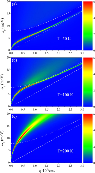
Figure 4. The momentum-dependent plasmon spectrum for (a) T = 50 K, (b) T = 100 K, and (c) T = 200 K. The up and low dashed curves in each panel indicate the interband and the intraband SPE boundaries, respectively. The color scale stands for the intensity of energy-loss function.
Download figure:
Standard image High-resolution image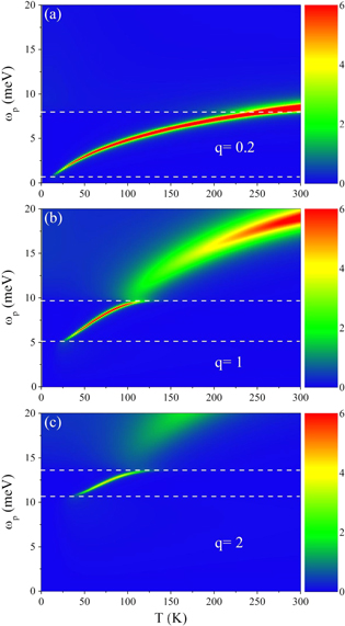
Figure 5. The temperature-dependent plasmon spectrum at (a) q = 0.2, (b) q = 1, and (c) q = 2. The up and low dashed curves in each panel indicate the interband and the intraband SPE boundaries, respectively. The color scale stands for the intensity of energy-loss function.
Download figure:
Standard image High-resolution image
The T-dependent plasmon excitation spectrum is shown in figure 5 for some chosen  . The smaller q is, the larger the ratio of intraband to interband transitions. Also, the difference in the excitation energy between them is enlarged. This directly reflects in the stronger dip (the weaker peak) in
  and the wider gap in
  . Consequently, a smaller q leads to a lower threshold temperature to induce the undamped plasmon mode (
 20 K for q = 0.2); furthermore, this plasmon mode can survive at higher
  . The opposite is true for a larger q. The possible existence range of the undamped plasmon mode, i.e. 25 K
  100 K at q = 1, is the same with the range that allows the coexistence of the intraband and interband-gap transitions, as depicted in figure 2(c). There exists a critical temperature (
 K for q = 1) through which the damped plasmon dominates the excitation spectrum. After that, the plasmon intensity grows with T monotonically. It should be noted that the existences of the two prominent plasmon modes at lower and higher temperatures both rely on the intraband transitions, because only the intraband transitions create the zero points in
  , as discussed in figure 1. The transformation from the undamped plasmon to the damped one is a discontinuous process over the change in temperature, which is manifested in their different occurrences and the different causes associated with them. The transformation happens when the plasmon frequency crosses the interband SPE boundary
  . Therefore, tracking the plasmon peak and observing the abrupt changes in its spectral width and dispersion when varying the temperature, one may obtain
  . In conjunction with the relation
  for low frequencies, the principal SOI term
  could be determined.
4. Conclusion
The Coulomb-excitation properties of monolayer silicene are studied by the tight-binding model and the random-phase approximation. The significant SOI in the buckled material opens up a sizable band gap. Accordingly, at certain temperatures, the intraband and the gap transitions coexist. The interplay between the two kinds of SPE channels could make one of the  zero points appear in the gap of
  , which gives rise to an undamped plasmon mode. There is a critical temperature through which the gap transition becomes insignificant and the intraband transitions turn into dominant. Then, the plasmon is damped by the interband absorption. It is shown that the crossover from the undamped plasmon mode to the damped one is a discontinuous process over the change in temperature, which illustrates the different occurrence mechanisms of them. This study points out the importance of the combined effects of SOI and temperature for low-frequency dielectric properties. The strong T-dependent characteristic excitations could mean a thermal way to manipulate the intrinsic plasmon in silicene. This may be of interest in the field of plasmonics. Other buckled honeycomb lattices, like germanene, could also exhibit similar excitation properties qualitatively.
Acknowledgment
This work was supported by the NSC of Taiwan, under Grant No. NSC 102-2112-M-006-007-MY3.