


Abstract
The strength of the light–matter interaction depends on the number of dipoles that can couple with the photon trapped in an optical cavity. The coupling strength can thus be maximized by filling the entire cavity volume with an ensemble of interacting dipoles. In this work this is achieved by inserting a highly doped semiconductor layer in a subwavelength plasmonic resonator. In our system the ultra-strong light–matter coupling occurs between a collective electronic excitation and the cavity photon. The measured coupling strength is 73% of the matter excitation energy, the highest ever reported for a light–matter coupled system at room temperature. We experimentally and theoretically demonstrate that such an ultra-strong interaction modifies the optical properties on a very wide spectral range (20–250 meV), and results in the appearance of a photonic gap of 38 meV, independently of the light polarization and angle of incidence. Light–matter ultra-strong coupling can thus be exploited to conceive metasurfaces with an engineered reflectivity band.
Export citation and abstract BibTeX RIS

Content from this work may be used under the terms of the Creative Commons Attribution 3.0 licence. Any further distribution of this work must maintain attribution to the author(s) and the title of the work, journal citation and DOI.
1. Introduction
When a material medium is inserted in an optical resonator, its interaction with light can be strongly enhanced and new quasi-particles can appear, the microcavity polaritons [1]. Their mixed light–matter nature has led to exciting applications in photonics, such as amplification [2] and low-threshold lasing [3]; all-optical devices with new functionalities [4–6] have also been demonstrated. The strength of the coupling is measured by the vacuum field Rabi splitting,  , which gives the energy separation between the microcavity polariton states when the cavity mode is resonant with the matter excitation energy,
  . When the coupling energy becomes comparable to that of the material excitation, the system enters a new quantum electrodynamics regime, the so-called ultra-strong coupling regime [7–9]. It has been first observed by coupling an electronic excitation in a quantum well (intersubband (ISB) excitation) and a microcavity mode [10, 11]. The quasi-particles issued from this coupling are the ISB polaritons [12]. Several other material systems have allowed the experimental observation of the ultra-strong coupling regime with a microcavity mode: superconducting circuits [13], cyclotron transitions [14], Frenkel molecular excitons [15], dye molecules [16]. The interaction between dye excitons and localized surface plasmons [17–19] has also led to the achievement of the ultra-strong coupling regime.
ISB transitions in quantum wells are a very interesting system for the observation of the ultra-strong coupling regime and the achievement of high values of the ratio between the Rabi and the matter excitation energy. Indeed,  and
and  can be both engineered: the first is controlled by the doping, while quantum wells can be designed in order to bring the transition energies towards the THz spectral range. In order to experimentally demonstrate the ultra-strong coupling regime with ISB polaritons, a large panel of parameters has been explored, in terms of cavity geometry, confining potential and doping, with the aim of maximizing the number of electrons involved in the interaction with the microcavity mode. The ultra-strong coupling has been first experimentally demonstrated in the mid-infrared by inserting 70 highly doped quantum wells in a planar microcavity [10]. It has then been observed in the THz frequency range, by using highly subwavelength cavities that are characterized by an extremely small effective volume [11]. A major breakthrough has been made by observing that the interaction with light can be strongly enhanced by increasing the doping and thus involving transitions between excited states of the quantum well. As dipole–dipole Coulomb interaction couples all the optically active ISB excitations, even if they have different frequencies, a unique collective mode is optically excited, the multisubband plasmon, concentrating the whole oscillator strength of the system [20, 21].
Figure 1 summarizes the measured values of the ratio between the Rabi and the matter excitation energies, the relative coupling strength  , which can be found in the literature (full symbols indicate room temperature results, while empty symbols refer to 4 K measurements) as a function of the width of the quantum well,
  . For
. For  nm, a single ISB transition is coupled with the cavity mode. The maximum relative coupling strength is in this case at most
  . The use of collective excitations (indicated as MSP in the figure) has allowed achieving a ratio
  greater than 0.5 at 4 K [20]. This increase of the relative coupling strength is associated with the uniform filling of the cavity mode volume with electrons. In this work, we further increase the strength of the coupling with respect to previous values in the literature by filling the entire cavity space with a highly doped semiconductor layer, in which all the oscillating dipoles contribute to the same collective excitation. We demonstrate that even though individual electrons are not confined in the semiconductor layer, the system displays a unique collective resonance, corresponding to the excitation of a confined plasmon, the Berreman mode [26–28]. By realizing a metasurface, based on an array of plasmonic microcavities with dimensions smaller than the wavelength, we demonstrate a ratio
  at room temperature. To the best of our knowledge, this value is not only the highest achieved with ISB systems, as shown in figure 1, but also the highest ever reported for a light–matter coupled system at room temperature. Indeed the only other systems displaying ultra-strong coupling regime at room temperature are based on organic molecules, for which the maximum value of
  attained is 30% [15, 16].

Figure 1. State of the art of the relative coupling strength  for intersubband systems as a function of the quantum well width. Solid symbols present room temperature results while empty symbols indicate 4 K measurements.
Download figure:
Standard image High-resolution imageA very interesting property of our system is that the ultra-strong coupling regime is accompanied by the appearance of a reflectivity band, whose width is determined by the density of the electron gas and by the geometry of the plasmonic microcavities. In our experiment, we measured a 38 meV photonic gap, hence larger than the phonon Reststrahlen band. Furthermore, due to the properties of the subwavelength cavities that we used, the reflectivity band is independent of the light polarization and angle of incidence. Light–matter strong interaction between an electronic polarization and an ensemble of sub-wavelength elements can therefore be used to realize new designer materials with specific dielectric properties [29].
This work is organized as follows. In section 2 we report the absorption spectra of increasingly wide quantum wells and demonstrate that they all display a single absorption peak, corresponding to the excitation of a collective mode. We present a model to calculate the dielectric function of the system, and demonstrate that the Drude dielectric function is recovered in the limit of increasing quantum well thickness. The crossover from the ISB plasmon to the multisubband plasmon up to the Berreman mode is then discussed, by distinguishing two contributions to the resonance energy, one associated with the electronic confinement and the other with the collective nature of the excitation. In section 3 we theoretically demonstrate that the ultra-strong coupling between a collective excitation of the electron gas and a microcavity mode results in the opening of a photonic gap in the polaritonic dispersion, with controllable width. We also show that a favorable system for achieving a wide reflectivity band is a microcavity completely filled with a doped semiconductor layer, displaying a Berreman mode. In section 4 we show that such Berreman mode has an optimized overlap with the microcavity photon, thus enabling the experimental achievement of a record value of the light–matter coupling at room temperature and the consequent profound modification of the optical properties of the system.
2. From multisubband plasmons to Berreman modes
In order to study the crossover from a multisubband plasmon to a Berreman mode, we realized four different samples, based on GaInAs/AlInAs quantum wells of increasing thickness  , from 18.5 nm to 148 nm. The quantum wells are highly doped, so that several subbands are occupied and thus several ISB transitions can be optically excited. By performing transmission spectra, we demonstrate in the following that all the samples display a unique optical resonance, even though the ISB transition energies progressively decrease when increasing the well thickness.
The four samples consist in  uncoupled Ga
 In
In As/Al
As/Al In
In As quantum wells, with thickness
  , grown on an undoped InP substrate by metal organic chemical vapor deposition. The quantum wells have the same nominal electronic density per unit volume (
 cm
cm ), while the number of quantum wells
  in the sample is chosen to keep constant the total length of interaction,
  (
( ). In this way the four samples are expected to show the same absorption amplitude, with different resonance energies, depending on the electronic confinement. The main characteristics of the samples are summarized in table 1, where we indicate the nominal quantum well and barrier width (
 and
and  , in nm), the number of quantum wells in the sample,
  and the number of occupied subbands at 0 K,
  .
.
Table 1.
Characteristics of the quantum wells used in our experiment. The first two columns give the nominal quantum well  and barrier
  width; the third column reports the number of quantum wells in the sample and the fourth presents the number of occupied subbands at 0 K.
  is the measured resonance energy at 300 K. N is the electronic density per unit volume in the well and γ the linewidth of each intersubband transition that we used in our model to reproduce the experimental spectra. The last two columns give the plasma energy,
  , and intersubband contribution,
  calculated at 300 K by taking into account the non-parabolicity.

|

|

|
N | γ |

|

|
||
|---|---|---|---|---|---|---|---|---|
| (nm) | (nm) |

|

|
(meV) | ( cm cm ) ) |
(meV) | (meV) | (meV) |
| 18.5 | 8 | 8 | 4 | 140.6 | 6.6 | 9.5 | 112.2 | 70.3 |
| 37 | 14.4 | 4 | 7 | 122.2 | 6.7 | 7.8 | 111.8 | 35.3 |
| 74 | 24 | 2 | 15 | 121.1 | 7.6 | 7 | 116.4 | 18 |
| 148 | 36 | 1 | 30 | 118.2 | 7.3 | 7.5 | 114.7 | 9 |
The samples have been prepared for transmission experiments, by mechanically thinning and polishing the substrate and by etching away the quantum wells from one part of the sample (as sketched in the inset of figure 2). Transmission measurements have been performed on the four samples at room temperature. The Globar lamp of a Bruker interferometer is focused on the sample using a parabolic mirror of focal length 10 cm. The transmitted intensity is measured by using a nitrogen cooled HgCdTe detector. In order to provide an electric field contribution along the growth direction and hence excite the ISB transitions, measurements have been performed at Brewster angle, at which the reflection on the surface vanishes [30]. The experimental geometry is sketched in the inset of figure 2. In order to isolate the quantum well contribution to the absorption, the transmission of the samples, measured in TM polarization (black line in the inset of figure 2), has been normalized by that measured, in the same polarization, from the part of the sample, where the quantum wells have been etched away (blue lines in the inset of figure 2). The absorption coefficient has been extracted from this measurement as  , where
  is the light propagation angle in the sample and T(E) is the normalized transmission [30]. The main panel of figure 2 presents the absorption spectra (continuous lines) extracted from transmission measurements at room temperature. A single resonance is observed for each sample, associated with a collective electronic excitation, at energy
  reported in table 1. The corresponding peak absorption coefficient is of the order of
  cm
cm . The full width at half the maximum (FWHM) of the absorption peak is comprised between 6% and 7% of the excitation energy, despite the high doping level and the strong non-parabolicity of the GaInAs/AlInAs material system. Note that in TE polarization no resonances are observed, but only an absorption background attributed to free carrier absorption.

Figure 2. Main panel: absorption spectra measured (continuous lines) and simulated (dashed lines) at 300 K. The total length of the absorbing medium is kept constant in the four samples, characterized by quantum wells of different thicknesses, by adjusting the number of quantum wells. The inset sketches the geometry used for measurements: the transmission through the sample (black line) at Brewster angle of a TM polarized beam from a Globar lamp is normalized to the transmission through the substrate (blue line).
Download figure:
Standard image High-resolution imageThe optical response of the system has been calculated through the z component of the effective conductivity tensor  , which includes the depolarization effects arising from the collective motion of electrons excited by an incident electromagnetic wave [31]. The ISB absorption coefficient is related to the conductivity tensor through the following expression:

where  is the refractive index of the material,
  the permittivity of the vacuum and c the speed of light. We calculated
  by taking into account the strong non-parabolicity of GaInAs/AlInAs material system. For this, each of the
  subbands has been divided into infinitesimal intervals
  , carrying a temperature dependent electronic density
  [32]. We associate to each transition
  in the momentum space a plasma frequency
  such that:
Here  is the oscillator strength of the transition
  , e the electron charge,
  the effective mass,
  the high frequency permittivity and
  the effective quantum well thickness renormalized by the Coulomb interaction [31]. The resulting conductivity tensor is:
where  is the frequency and
  is the FWHM of the
  transition.
Dashed lines in figure 2 present the absorption spectra calculated at room temperature for the four samples by using equation (1), with  obtained from equation (3). We used the same FWHM for each ISB transition. The values γ that allowed us to fit the observed linewidths are reported in table 1. The electronic density in the well, N, was adjusted to reproduce the observed resonance energy
  and it is reported in table 1. These values are very close to the nominal electronic concentration. Note that the absorption coefficient in cm
 is automatically obtained by our calculation and is in very good agreement with the experimental one.
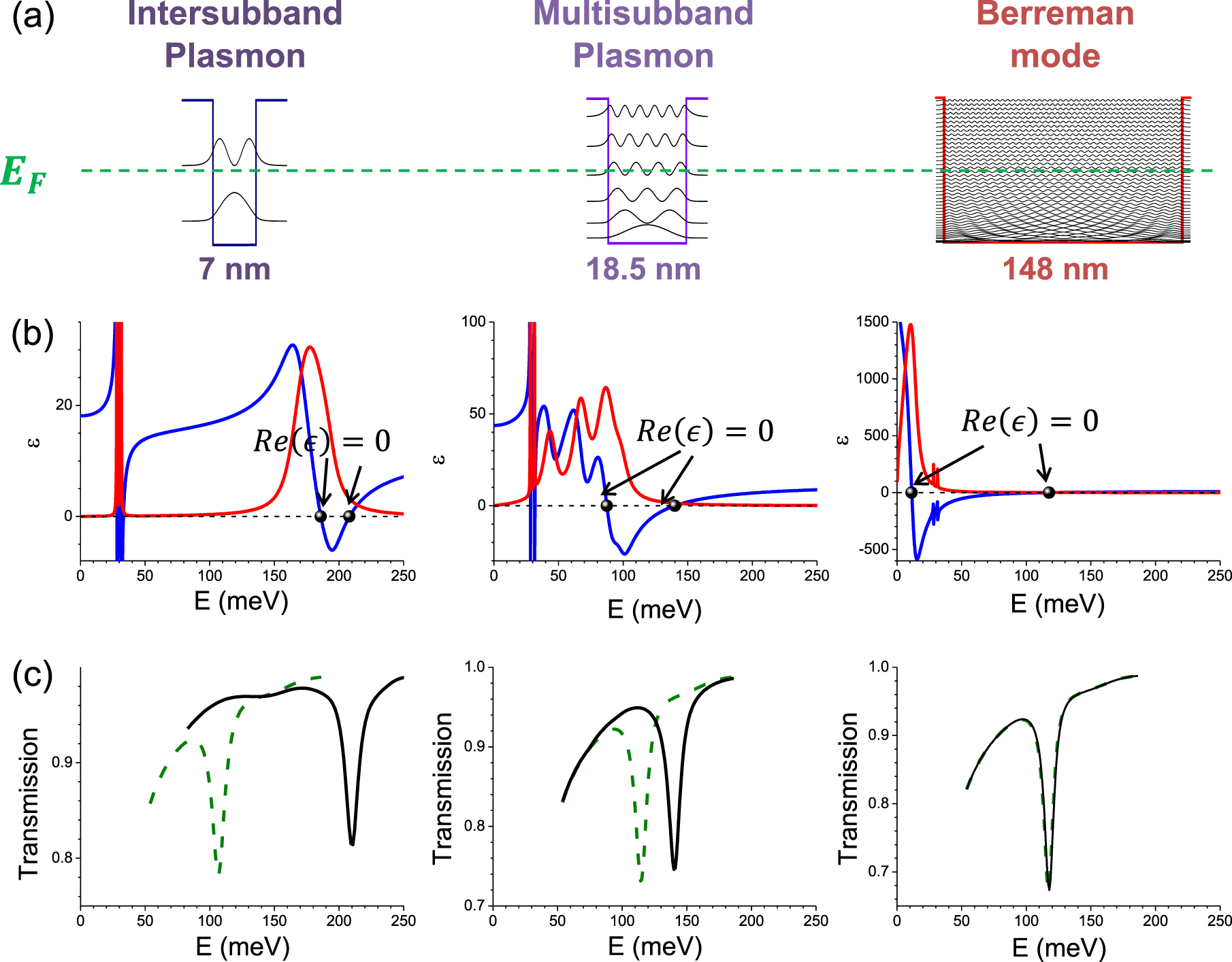
It is important to note that even though the four absorption spectra presented above are similar, as they all display a single sharp absorption resonance, the microscopic nature of the physical systems is progressively changed. Indeed, by increasing the quantum well width, the number of occupied subbands increases and the transition energies tend to zero. This is shown in figure 3(a), where we plotted the band diagrams and the square moduli of the electronic wavefunctions for three GaInAs/AlInAs quantum wells of thickness 7 nm, 18.5 nm and 148 nm and with similar electronic density (from left to right:  cm
cm ,
,  cm
cm ,
,  cm
cm ). The Fermi energy at 0 K is indicated in the figure by a dashed line. By increasing the quantum well thickness, the number of occupied subbands is increased and hence more and more transitions are optically excited. The progressive crossover from an ISB transition, to a multisubband plasmon, up to a Berreman mode is studied by calculating the complex permittivity of the system,
  . In the semiclassical model presented above, it is given by:
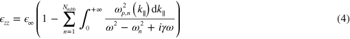
Figure 3(b) presents the real (blue line) and imaginary (red line) part of the complex permittivity calculated for a 7 nm, 18.5 nm and for a 148 nm quantum well at room temperature. The real part of the permittivity has two zeros, indicated by a bullet in the figure. One zero is at the optical resonance,  , while the second one is at lower energy. When a single ISB transition is optically active (as in the 7 nm quantum well) this second resonance is close to the energy of the bare ISB transition. If several subbands are occupied, it can be considered as an indication of the ISB contribution to the energy of the optical resonance, decreasing when
  increases. In the following we introduce an expression for this ISB contribution, indicated as
  and written in terms of the transition energies. The imaginary part of the dielectric function is maximum at an energy close to that of the ISB transition in the 7 nm quantum well case, while several maxima can be observed when several ISB transitions are optically excited. When the transition energies tend to zero, like in the case of the largest quantum well, a single maximum is observed again, at an energy that can be related to an effective ISB contribution. Note that the dielectric function of the 148 nm quantum well is very similar to that of a free electron gas, described by the Drude model (except for the divergency at zero frequency). In order to better evidence this point, we simulated, by using a commercial Finite Elements solver, the transmission through the doped semiconductor layer at Brewster angle and in TM polarization. The dispersion due to the doped layers was included in the simulation by using equation (4) (continuous line) and Drude model for comparison (dashed line). The Drude model gives a transmission polarized in the direction perpendicular to the layers at the plasma energy. This polarization selection rule is a characteristic of the Berreman effect [26–28], and it has been observed for doped semiconductor thin films. The results presented in figure 2 and the calculation in figure 3 therefore show the progressive crossover from a multisubband plasmon, governed by the quantum confinement of the GaInAs/AlInAs well/barrier system, to a Berreman mode, which corresponds to a three dimensional confined plasmon. Our model recovers the results obtained by Drude model for the largest quantum well and it is hence suitable to describe all the three regimes discussed in figure 3.
Figure 3. Crossover from an intersubband plasmon to a Berreman mode. Panel (a) presents the band diagram and square moduli of the wavefunctions of three GaInAs/AlInAs quantum wells, of thickness (respectively electronic density) (from left to right) 7 nm ( cm
cm ), 18.5 nm (
 cm
cm ) and 148 nm (
 cm
cm ). The Fermi energy at 0 K,
  is indicated by a dashed line. In panel (b) we show the real (blue line) and imaginary (red line) part of the dielectric function calculated by using equation (4) for the three quantum wells. Panel (c) presents the calculated transmission by using equation (4) (continuous line) and that obtained with Drude model (dashed line). The simulation has been performed by using a commercial Finite Elements solver, by calculating the transmission through the doped semiconductor layer at Brewster angle and in TM polarization. A total semiconductor thickness of 148 nm has been considered for the three simulations.
Download figure:
Standard image High-resolution imageThe crossover from the ISB plasmon to the Berreman mode can be also clearly seen analytically, by observing that the absorption resonance,  has in general two main contributions, one related to the electronic confinement, the other expressing the collective nature of the excitation. Indeed it is possible to introduce an effective plasma frequency [21], associated with the bright multisubband mode, by adding all the contributions from the ISB transitions
  involved in the interaction with light
4
:
involved in the interaction with light
4
:

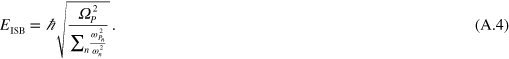
As demonstrated in the appendix, the resonance energy can be written as:

where the ISB contribution,  , is the harmonic mean of the squared ISB transition energies weighted by their plasma energy:
The calculated effective plasma energies and ISB contributions (in meV) for the four samples studied in this work are presented in the last two columns of table 1. We can clearly see that, when increasing the quantum well width and hence the number of occupied subbands, the ISB contribution progressively decreases and becomes a negligible fraction of the resonance energy. Note that equation (6) is formally identical to the usual expression of the depolarization shifted energy for a single ISB transition. As a consequence the limit for a negligible plasma energy as compared to the ISB contribution is also recovered by our model.
3. Multisubband plasmons for ultra-strong coupling regime: theoretical description
When a cavity mode is brought into resonance with the multisubband plasmon, the system enters the ultra-strong coupling regime, with a Rabi energy  [21], where
  is the overlap between the photon mode and the matter polarization [11]. As the microscopic dipoles associated with the electronic excitations are oriented along the growth direction z, it can be calculated as the ratio between the electromagnetic energy contained in the z-component of the field in the quantum well region and the total electromagnetic energy:
Here  is the displacement vector and the integral at the numerator is intended on the quantum well volume, while that at the denominator is on the entire volume of the system.
The resulting polariton dispersion is described by the following secular equation, issued from the diagonalization of the light−matter Hamiltonian in the dipole gauge [11, 21, 33]:

where  is the cavity mode energy. Figure 4 presents the polariton dispersion, normalized to the matter excitation energy,
  , plotted for different values of
  . From these curves we can see that the polaritonic dispersion, and particularly the shape of the lower polariton branch, is significantly modified by the increase of the ratio
  . Indeed, while the horizontal asymptote of the upper polariton branch is
  , that of the lower polariton branch is
  . This means that the lower branch can be pushed at arbitrarily low frequencies by increasing the coupling, thus ensuring strong absorption strength even in the far infrared. Furthermore, a photonic gap appears in the dispersion, whose width is given by:
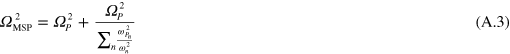
The increase of the photonic gap as a function of the ratio  is shown in the inset of figure 4. The properties of the photonic gap can be adjusted by modifying
  through the overlap with the cavity mode (
 ) and the density of the electron gas (which affects
  ).
).

Figure 4. Main panel: energy of the polariton branches as a function of the energy of the cavity mode, normalized to the matter excitation energy ( ). Four dispersion curves are shown, corresponding to different relative coupling strenghts. Inset: energy of the polaritonic gap normalized to the matter excitation as a function of the relative coupling strength.
Download figure:
Standard image High-resolution imageThe Berreman mode studied in the previous section optimizes the overlap between the electronic polarization and the light mode,  , as the cavity volume can be completely filled with a highly doped semiconductor layer. It is hence ideal for achieving the ultra-strong coupling regime, thus opening a wide polaritonic gap.
4. Ultra-strong coupling and artificial Reststrahlen band
In order to observe the ultra-strong coupling regime and to experimentally evidence the reflectivity band, we coupled the Berreman mode with the photonic mode of a highly subwavelength cavity, based on a metallic confinement [34–37]. We used the sample with  , already presented in section 2. After Ti/Au (10/500 nm) metallization of the surface of the sample, the last was epoxy-bonded on a host InP sustrate, on top of which a Ti/Au layer was deposited. After substrate removal, e-beam lithography and Ti/Au metallization were performed to pattern the surface of the sample with an array of gold square patches. Figure 5(a) presents a sketch of the sample with an optical microscope image of the array on top. The total thickness of the cavity is 240 nm. The size s of the square patches defines the energy of the cavity modes, while the periodicity of the array p impacts the coupling efficiency with the free space radiation. In order to vary the detuning between the cavity and the Berreman modes, we realized square patches of different sizes, varying from s = 0.65 μm, confining the fundamental mode at
  , to
, to  , corresponding to
  . The distance between the patches, o, is kept constant and equal to
  . Figure 5(b) presents a simulation of the electric field for the fundamental mode (for
  ). Note that the optical resonances of this kind of cavities can be excited independently of the light polarization [37]. Furthermore, the resonance energy is independent of the angle of incidence [37]. The calculated overlap factor between the quantum well and the cavity mode is
  . This value is mainly limited by the thickness of the AlInAs barriers and by the metal losses in the mid-infrared region.
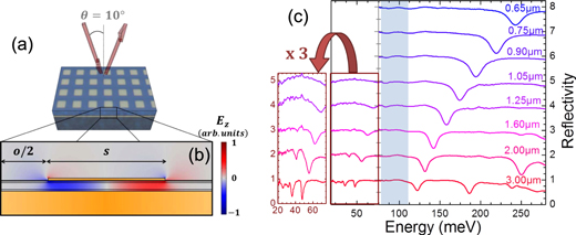
Figure 5. (a) Sketch of the sample, with on top an optical microscope image of the subwavelength grating. The cavity thickness is 240 nm. The gold patches have a width  and they are separated by a distance
  . (b) z-component of the electric field for the fundamental mode in the case of the
  cavity. (c) Set of chosen reflectivity spectra, offset for clarity, of the array of patches measured at room temperature, in the geometry sketched in panel (a). The brown rectangle indicates the part of the spectra that has been detected by a bolometer. In order to better evidence the reflectivity minima, the left part of the figure shows a zoom where the signal has been multiplied by a factor of three. The magnified spectra have also been translated in order to keep the same baseline as in the right part of the figure.
Download figure:
Standard image High-resolution imageReflectivity measurements have been performed at room temperature, at an incidence angle of  , as sketched in figure 5(a). The Globar lamp of a Bruker interferometer is focused on the sample and the reflected intensity is measured by using two different detectors, to access a wide spectral range: a 4.5 K Si bolometer (20–75 meV) and a nitrogen cooled HgCdTe detector (75–300 meV). The measured reflectivity spectra are then normalized to those obtained on a reference sample, made of a gold plane. A set of measured spectra, offset for clarity, are shown in the main panel of figure 5(c). The separation between the two spectral ranges, obtained with the two detectors, has been evidenced in the figure. Note that no corrections have been applied to the baselines of the spectra. The contrast of the reflectivity minima is close to 0.8 for high energy modes, but it progressively decreases in the far infrared, due to a spillover of the cavity mode on the metallic surface. In order to better evidence the reflectivity resonances in the THz part of the spectra, the reflectivity signal has been magnified by three, as it is presented on the left side of the figure. It shows that, even in the THz part of the spectra, the resonances are very well defined, with a very good signal to noise ratio. Looking from the top of figure 5(c), one can observe the upper polariton resonance decreasing in energy from 245 meV for
  to 120 meV for
  . In the lower spectra shown in the figure there are energy minima beyond the upper polariton which are associated with the coupling between the Berreman and the third order cavity mode. For these same spectra the lower polariton couples to the phonon Reststrahlen band and, therefore, several reflectivity minima are visible in the low energy part of the spectra. The light-blue region in figure 5(c) delimits a range in which, for all metallic patches, the reflectivity is one. This region is the photonic gap of the polaritonic dispersion.
In order to extract the polaritonic dispersion from the minima of the reflectivity spectra, we measured the reflectivity of cavities with the same thickness as the previous ones but filled with an undoped GaInAs layer. In this way we measured for each s the bare cavity resonances,  . Figure 6(a) presents the reflectivity minima (bullets) as a function of the first order cavity mode energies. The ultra-strong coupling with the Berreman mode results in the opening of a wide reflectivity band, delimited by the horizontal asymptotes of the upper and lower polariton branches. The Berreman mode energy, indicated by a star in figure 6, fixes the upper bound of the polaritonic gap. The lower bound occurring at high cavity energy is given by
  . From the data we extract
 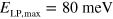 and thus a vacuum Rabi energy
 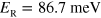 , corresponding to 73% of the matter excitation energy (
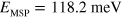 ). Both this Rabi energy and the ratio
  are the highest measured for ISB polaritons. Furthermore the ratio between the Rabi and matter excitation energy is the highest achieved at room temperature of all quantum systems. When the lower polariton branch approaches the energies of GaInAs and AlInAs optical phonons, more anticrossing features are visible, demonstrating the existence of phonon–plasmon–polariton modes.
Figure 6. (a) Energy position of the reflectivity minima as a function of the fundamental cavity mode energy (bullets). The star indicates the energy of the Berreman mode as measured in transmission at Brewster angle. The blue lines present the simulated polaritonic dispersion by including the coupling with optical phonons. For comparison, the dashed grey line presents the simulated dispersion by only including the coupling between the Berreman and the cavity mode. (b) Simulated effective index of the optical modes in presence of the coupling with the Berreman mode (blue continuous lines) and, as a comparison, for an undoped GaInAs layer (red dashed lines). The shaded regions present the reflectivity bands of the artificial material.
Download figure:
Standard image High-resolution imageWe simulated the reflectivity spectra by using a Finite Elements commercial solver, by taking into account the geometry of the cavities, the permittivity of the multisubband plasmon (equation (4)), the dispersion of the optical phonons and that of the Au layers [38]. The optical phonon dispersion has been included in our simulations as a two-pole dispersion relation for each of the ternary alloys [39]:
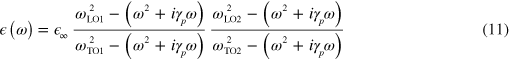
where the suffixes LO and TO refer, respectively, to the longitudinal and the transverse optical phonon frequency of the two bulk binary semiconductors 1 and 2 forming the ternary alloy layers. A phenomenological broadening of the phonon modes  has been introduced. This value is of the same order of magnitude as the optical phonon anharmonic decay [40]. The solid blue lines in figure 6(a) present the simulated polaritonic dispersion, in excellent agreement with our data. Note that, as the cavity mode has an overlap also with the AlInAs layers, we observe a coupling of the cavity mode with the optical phonons of both ternary alloys. As a comparison, the grey dashed line presents the dispersion calculated without taking into account the coupling with the optical phonons. It has the same shape as the theoretical dispersion curves discussed in relation with figure 4, with a single anticrossing due to the interaction with the Berreman mode.
Figure 6(b) presents the calculated effective index dispersion of the optical modes (solid line) for our structures in comparison to that of identical cavities but filled with a GaInAs undoped layer (dashed line). Two reflectivity bands are apparent from the illustration: the low energy is the usual one associated with the optical phonons, while the second, centred around 100 meV, is due to the coupling of the cavity modes with the collective excitation of the doped well. Note that for the undoped layer only the phonon reflectivity band is visible. The 'plasmonic' reflectivity band is 38 meV wide, thus more than twice wider than the energy band of the optical phonon. Furthermore, the plasmon induced reflectivity band is not only much larger than the phonon Reststrahlen band, but it can be engineered by playing on both the doping concentration and the profile of the optical mode. Due to the properties of the metal-dielectric-metal cavities used in this work, it is also independent of the polarization and incidence angle of the light [37].
In conclusion, by combining the properties of subwavelength plasmonic cavities and collective excitations of heavily doped layers, we achieved an unprecedented ultra-strong coupling regime at room temperature. The polaritonic dispersion is characterized by the appearance of a wide photonic gap, which can be exploited to realize artificial materials described by unconventional dielectric function. Furthermore, the ultrastrong interaction pushes the lower polariton branch towards the THz range, thus transferring in the THz a part of the huge interaction strength achieved in the mid-infrared. This phenomenon could be exploited to design room temperature THz devices driven by a mid-infrared excitation of the matter.
Acknowledgements
We acknowledge financial support from the ERC grant 'ADEQUATE' and from the French RENATECH network.
Appendix.: ISB contribution to the multisubband plasmon energy
Let us consider a highly doped semiconductor quantum well with one or several occupied subbands, displaying a single absorption resonance. If the subbands are parabolic, and the losses are neglected, the dielectric function can be written as:

where  and
and  are respectively the plasma energy and the frequency of the transition
  . The absorption spectrum taking into account the depolarization effect is then calculated, as discussed in section 2, by considering the imaginary part of
  . If a single resonance is present at frequency
  with an effective plasma frequency
  , the resulting response of the system is given by:

The equivalence between expressions (A.1) and (A.2) of the dielectric functions is valid for all frequencies and in particular at  . In this case we get:
This allows us to define an effective ISB energy as the harmonic mean of the ISB transition energies, weighted by their plasma frequency:
The collective excitation energy is thus written as: 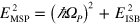 .
.
Footnotes
- 4
In order to simplify the notation, we consider here parabolic subbands. In the numerical calculations, non-parabolicity has been included in the expressions of
 and by integrating over the subband dispersions like in equation (2).

