


Abstract
Silicene is a 2D topological insulator due to its fairly large spin–orbital interaction and features a buckled lattice structure that allows one to control the effective mass of Dirac electrons by a perpendicular electric field. We propose the use of a spatially alternative electric field to generate multiple topologically-protected interface states (TIS) in the bulk silicene. It is shown that when the valley-dependent electron mass (defining the Chern number of an insulating bulk silicene) changes its sign or discontinues due to spatial variation of the electric field, multiple TIS appear in the insulating bulk silicene. The TIS come from the K and  valleys and sustain dissipationless valley or spin–valley-dependent currents, which are immune to both the valley-conservation and spin-observation scattering. It is also found that the coupling among TIS due to spatial electron tunneling excites the TIS, and whether there is an excitation gap or not depends on the even or odd TIS number. Our findings may shed light on manufacturing topological electron devices.
Export citation and abstract BibTeX RIS

Content from this work may be used under the terms of the Creative Commons Attribution 3.0 licence. Any further distribution of this work must maintain attribution to the author(s) and the title of the work, journal citation and DOI.
1. Introduction
A topological insulator [1–4], as a new state of quantum matter, has tremendous interest to both fundamental condensed matter physics and potential applications in spintronics as well as quantum computation. A topological insulator is insulating in the bulk due to a direct bulk band gap, whereas on the boundary there are topologically protected gapless surface or edge states that are immune to nonmagnetic disorder due to the time reversal symmetry. The first experimental realization of a topological state was performed in the HgTe/CdTe sandwiched quantum well, [2] where HgTe is an inverted-band material, and CdTe has a normal band structure. Although Kane and Mele [1] first predicted the quantum spin Hall insulator (QSHI) in the graphene system with an intrinsic spin–orbital interaction (SOI), the experiment observation is still lacking due to very weak SOI in graphene.
Researchers began to focus on other 2D crystals with the graphene-like lattice structure but a stronger SOI, such as silicene [5–13],  [14–17], and germanene [5]. Silicene, a single layer of silicon atoms with the honeycomb lattice structure, seems more attractive since the silicon-based semiconductor electronics is very mature and dominates the semiconductor industry. In experiment, Vogt et al [6] successfully synthesized the single-layer silicene and confirmed the predicted electronic structures and properties by measurement of scanning tunneling microscopy and angular-resolved photoemission spectroscopy. The density functional computation [5] showed that the SOI strength in silicene amounts to 1.55 meV and can be further enhanced by strain. Besides the sizeable SOI, another salient feature of silicene is the buckled lattice structure that the A and B sublattices are not in the same plane unlike graphene, so the inversion symmetry can be broken by using a perpendicular electric field resulting in a staggered potential. Therefore, the energy gap or effective mass of low-energy Dirac electrons in silience can be controlled electrically. When the energy gap opened by the staggered potential is larger than the SOI strength, silicene is transitioned to a quantum valley Hall insulator (QVHI) from a QSHI [11], but no edge states at the boundary of silicene are observed since the valley degree of freedom is ill-defined in vacuum.
As is known, the helical edge states in a QSHI are topologically protected by the time reversal symmetry and support dissipationless electron transport, so they are very useful for manufacturing dissipationless electron devices. However, having only two conductive channels and only residing at the boundaries of the 2D QSHI may limit their application to dissipationless electronic devices. Therefore, it is desirable to transfer the edge states into the bulk of materials and construct multiple topologically-protected conductive channels. The silicene may fill this blank with the help of an inhomogeneous electric field or gate voltage. As Ezawa [18] pointed out in a recent work, the bulk-boundary correspondence for a QVHI is seen in the middle of silicene, where the nonzero electric field discontinues to define an interface state that is topologically protected and robust against disorder scattering.
In this paper, we develop Ezawaʼs model [18] to engineer multiple topological interface states (TIS) in the bulk of silicene by using a spatially alternative electric field and detailing the properties of the TIS. It is shown that, like the helical edge state, the TIS is born wherever the two insulating phases with different Chern numbers connect to each other and the energy gap closes. The K and  electrons constitute the TIS while electrons in the helical edge state in a QSHI are from the X point. The electron velocity in the former case is much larger than the latter one. The coupling among the TIS due to spatial electron tunneling may or may not lead to an excitation gap, and this depends on the even or odd TIS number. The pure dissipationless valley currents or spin–valley-dependent currents are flowing in the TIS, which are immune to not only moderate nonmagnetic disorder but also long-range disorder regardless of magnetic or nonmagnetic ones.
The rest of this paper is organized as follows. In section 2, we present the model and introduce the properties of silicene in a uniform electric field. In section 3, we first detail the TIS sustaining pure helical valley currents without the SOI and present the band structure of a silicene ribbon to describe them. In the following section, we turn on the SOI to address the TIS with spin-valley dependent currents, and the disorder effect on the TIS is also studied. A conclusion is drawn in the last section.
2. Model
Similar to the graphene lattice structure, silicene consists of the honeycomb lattice of silicon atoms with two sublattices made of A and B sites. However, it has a buckled structure [5] that the two sublattice planes are separated by a distance l as schematically shown in figure 1. Within an external electric field  , a staggered sublattice potential
  between silicon atoms at A sites and B sites is generated, and it can induce a controllable energy gap of the low-energy particles at both K and
  valleys. In this study, we assume that a spatially alternative electric field
  in figure 1 is applied to the silicene system, the magnitude of
  may remain the same but the direction of
  is alternative. This is feasible in experiment by designing a staggered gate voltage based on photo lithography. We employ a tight-binding model of the π orbits of silicon atoms to describe system and the Hamiltonian is given by [18]

where  (
( ) is the electron creation (annihilation) operator at site i with spin polarization α(β),
 denotes the summation over the nearest (next-nearest) neighbor lattice sites. The first term describes the π-orbit hopping among the nearest neighbor sites with the hopping integral t. The second term stands for the effective SOI term with the strength λ,
  (
( ) is the Pauli matrix.
  if the next-nearest-neighboring hopping is anticlockwise and
  if it is clockwise with respect to the positive z axis. The third term represents the staggered lattice potential
  induced by the site-dependent electric field
  , where
  for the A (B) site. It is noted that the Rashba SOI is neglected here since its strength is an order of magnitude smaller than the SOI strength λ.
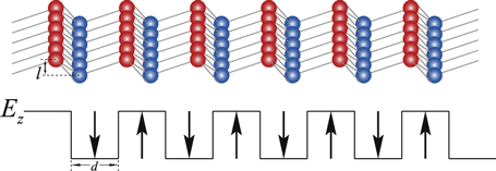
Figure 1. Schematic of silicene with the buckled lattice structure. A spatially alternative electric field  is assumed perpendicular to the silicene plane. The
  direction is alternatively reversed, l is the A and B sublattice distance, d is the spatial periodicity of the oscillating
  .
.
Download figure:
Standard image High-resolution imageBy projecting equation (1) into the momentum space and then expanding it at K and  points, one can obtain the following low-energy effective Dirac-type Hamiltonian with a uniform staggered potential
  assumed

where  is the valley label for the two opposite valleys K and
  ,
,  is the x(y)-component momentum of particles. The matrices
  and
and  (
( ) are the Pauli matrices, and the former acts on the pseudospin space associated with the A and B sublattices, while the latter is for the real spin.
  is the Fermi velocity with a = 3.86 Å being the lattice constant [5].
The spin and valley-dependent eigenvalues can be evaluated from the Hamiltonian above

where  and
and  are respectively the valley and spin indices. An energy gap is opened by both the SOI and the staggered potential
  , which also defines the effective mass of Dirac fermions as

and it is spin and valley dependent. The staggered potential  also plays an important role in determining the sign of mass. One can obtain the Chern number to classify an insulator by summing up Berry curvatures of the occupied bands in the momentum space,

where  is the spin and valley-dependent Berry curvature and
  is the periodic part of the Bloch function and n is the band index. When the Fermi energy resides in the energy gap
  , the parameter-dependent Chern number was found to be

For a uniform silicene described by the Hamiltonian above (equation (2)), the Chern number is zero  , since the time reversal symmetry is preserved. Meanwhile the spin or valley Chern number may be nonzero and can be used to characterize the system,
  and
and  , which depends on the relative strength of
  and λ. When
  ,
,  and
and  , the system is actually a QSHI with conductive channels at the boundary of system (helical edge states). Whereas for the opposite case,
  ,
,  and
and  depending on the sign of
  , and the system transitions to a QVHI as studied by Xiao et al in [19].
It is seen there is a quantum phase transition [11] by increasing  through the electric field
  and the critical point is at
  , where the energy gap closes
  . In the real space, there will be a conductive interface channel dividing the QVHI and QSHI regions if the
  could be controlled deliberately in each region through the electric field. Although the QVHI looks like a band insulator by itself, there is no conductive edge states unlike the QSHI. The reason is that the valley degree of freedom is crucially related to the honeycomb lattice structure and defined in the momentum space, and it will be ill-defined in the nonhoneycomb lattice materials or vacuum. Alternatively, the valleys are severely mixed in the nongraphene lattice structure. While for the charge or spin degree of freedom, the vacuum could be regarded as the C = 0 or
  insulator, thus the chiral edge states in a quantum Hall insulator or helical edge states in a QSHI represent the quantum phase transition in real space where the band gap is closing. Therefore, it is expected that in the bulk of silicene, an inhomogeneous
  should produce different quantum phases characterized by
  , and the interface connecting the two neighboring quantum phases will be conductive and topologically-protected. In the following sections, we will discuss in detail the properties of the TIS constructed by a spatially alternative electric field applied in the silicene system.
3. Valley helical interface states
For simplicity, we first neglect the SOI in silicene ( ) and only consider the nonuniform staggered potential
  effect, i.e., the spin degree of freedom is temporarily assumed degenerate if not stated otherwise. The mass of Dirac electrons in equation (4) becomes spin-independent
  , so the spin Chern number
  but the valley Chern number
  depending on the sign of
  , which in turn is determined by the direction of
  . As noted above, to see the boundary state of the QVHI, one need construct a boundary or interface where the valley Chern number discontinues or reverses its sign.
We construct a single interface in silicene by reversing the electric field direction,  at
at  and
and  at
at  , as schematically shown in figure 2(a). This leads to the opposite staggered potential
  in the two regions. The interface is at y = 0 and the system is uniform along the x axis. By solving equation (2) with
  , the wavefunctions in the energy gap
  are given by
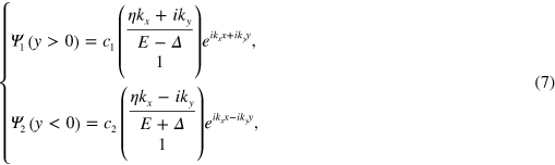
where  (i = 1, 2) are the undetermined coefficients,
 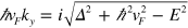 ,
,  is assumed to be conserved when the wavefunctions are scattered at the interface y = 0. Note the wavefunctions in the energy gap are evanescent and different in the two regions due to the opposite staggered potential
  . Since the wavefunctions are continuous at y = 0,
  and one can obtain the meaningful solution to the secular equation of its coefficient matrix,

by neglecting the other solution  . Note we only focus on those in the energy gap
  . It is seen that such interface states have a definite chirality and the K and
  valleys have opposite one, so they can be referred to as the helical TIS like the helical edge states in a QSHI. A pure valley current flows along the interface at y = 0 as plotted in figure 2(a), and it is topologically protected and robust against the valley-conservation scattering. Different from the helical edge states, the electrons in this helical interface state are from the K (
 ) point and have the Fermi velocity
  of the silicene unlike the helical edge state [19]. Therefore, this single interface state can provide a single fully valley-polarized conductance, which is also one of the central issues in the field of valleytrocis (valley electronics) [20–25].
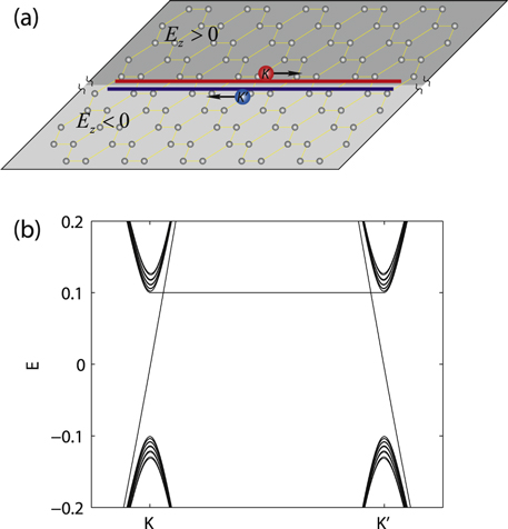
Figure 2. (a) Schematic of an interface constructed in silicene between  and
and  . A pure valley current is flowing at the interface since the K and
  electrons move oppositely due to the definite chirality. (b) Band structure of a zigzag silicene ribbon with an interface inside the ribbon. The interface is exactly at the middle of the ribbon and other parameters are described in text.
Download figure:
Standard image High-resolution imageTo further clarify the TIS, we calculate the band structure of an infinite zigzag silicene nanoribbon with  at
at  , and
, and  at
at  , where L is the width of the ribbon. In our calculations, parameters are taken as t = 1.0 eV,
  , the zigzag chain number of the ribbon is taken 450 and thus
  nm. It is seen in figure 2(b) that there are two subbands in the energy gap
  with the linear E-
 relation crossing the Fermi energy
  at the K or
  point, while other subbands show an energy gap
  . So a single Dirac cone composed of both the K and
  valleys resides in the gap. The TIS here connect the
  region to the
  region, so the energy gap is closed at the interface. The TIS can also be regarded as the bulk-boundary correspondence for a QVHI [18]. It is noted that such a single TIS could be constructed in a finite-size silicene without periodic conditions and there is a net pure valley current flowing in the system as plotted in figure 2(a). This is in stark contrast to the spin helical edge states in a QSHI, where the edges states appear in pairs and no net pure spin current flows in the system.
An interesting question arises where the pure valley current relaxes for a single interface builded in silicene. As mentioned above, the valley degree of freedom comes from the band structure of the honeycomb lattice materials and is defined in the momentum space, so near the boundaries of silicene, the K and  valleys gradually lose their definition due to the boundary effect; alternatively, the two valleys are severely mixed. This indicates that the pure valley current flowing along the middle interface will relax gradually toward the boundary of the system due to the valley-mixing scattering. Actually, because of the finite-size effect of the ribbon, the zero-energy interface state does not exactly reside at
  in figure 2(b). However, the derivation is negligibly small and inversely proportional to the ribbon width L.
The single interface inside silicene reminds us that it is possible to engineer multiple TIS with the help of a spatially alternative electric field in figure 1. Certainly, their excitations cannot be neglected due to the electron tunneling between neighboring states, and this question is the same as the finite-size effect that excites a gap in the helical edge states of a QSHI [26]. For simplicity, we discuss first the two interfaces in silicene defined by  at
at  ,
,  at
at  , and
, and  at
at  , so the two interfaces locate at y = 0 and y = d, respectively. Similar to equation (7), we present the wavefunctions in each region as
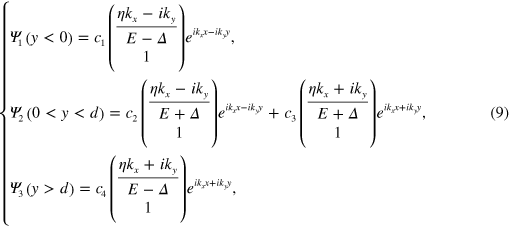
where  are the undetermined coefficients. Similarly, from the continuum conditions of wavefunctions at y = 0 and y = d, one can obtain the following transcendental equation for the interface states in the energy gap
  ,
,

The analytical solutions can be worked out at two extremes,  and
and  . The first is the distance d of the two interfaces much larger than the lattice constant a, and thus the coupling between neighboring interfaces can be neglected, so the solutions go to equation (8); the second limit
  results in the minimum excitation gap at the
  point
point  with
with  , where the damping length
  , so a larger electric field
  will produce a smaller damping length so as to a smaller excitation gap, which is favorable to engineer multiple topological conductive channels.
The two interface states have the opposite chiralities, which can be seen from the solutions of equation (10)  with
with  . Hence, the pure valley current in each interface is flowing oppositely to each other. Such a pair of interface states like the helical edge states can form a self-close path with pure valley current flowing, which is schematically plotted in figure 3(a). This case is exactly same as the helical edge state in a QSHI sustaining a dissipationless spin current along the boundary of the system. The electric fields inside and outside the close-path in figure 3(a) are opposite and the valley Chern number changes its sign across the interface, as a result, the connection should support a valley current. Certainly, the honeycomb lattice outside the circle is vitally important to define the valley degree of freedom.
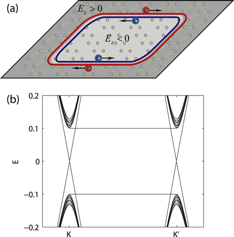
Figure 3. (a) Schematic of a circular interface constructed in silicene connecting  and
and  regions. A pure valley current is flowing at the circular interface. (b) Band structure of a zigzag silicene ribbon with the two interfaces constructed in the middle of ribbon.
  and
and  .
.
Download figure:
Standard image High-resolution imageWe also compute the band structure of an infinite silicene ribbon with two interfaces by reversing  twice, and the numerical results are plotted in figure 3(b). It is shown that there are two Dirac cones at the K and
  points in the energy gap
  . At each valley, two bands in the energy gap with opposite chiralites come respectively from two interfaces. Similarly, at each interface, the chiralities from the two valleys are also opposite. This leads to the pure valley current in each interface flowing oppositely. It is also shown there is a small energy excitation gap at Dirac cones as shown in figure 3(b). As explained above, it comes from the coupling between the two interfaces due to the electron tunneling.
We proceed to examine the multiple TIS in silicene created by the spatially alternative  as plotted in figure 1, where the magnitude of
  is assumed to be unchanged but the direction is reversed. The coupling among the multiple TIS will further modify the excitation spectrum in the energy gap
  , however, the maximum of the excitation gap has the same order as that of the two interface state case in equation (10),
  . Actually, one can consider safely a nearest-neighboring coupling model since the next-nearest-neighboring coupling of the two interface states is exponentially smaller, so the excitation-gap spectrum at the
  point approximates

where  is similar to a wavevector with the integer n and
  . Therefore, one can see the minimum excitation energy
  when the interface number is odd
  with v being an integer; while the interface number is even,
  , the minimum excitation energy is
  and there must an energy gap in the excitation spectrum
  . This even–odd effect of the excitation spectrum will be further confirmed by numerical calculations in the following. In the above equation the periodical alternative
  and the equal length d are implicitly assumed. It is also seen that a stronger electric field
  or larger periodicity d is necessary to avoid a large excitation gap.
The band structure and conductance of a silicene ribbon are presented in figure 4 for different interface numbers,  and
and  . A serial of TIS appear in the energy gap
  , all of them are topologically protected and each of them sustains a valley-dependent current. Comparing figures 4(a) to (c), we can see that for the odd number of interfaces at
  , there must a band crossing the Fermi energy
  whatever the magnitude of d and
  ; whereas for the even number of interfaces at
  , there must exist an excitation gap residing at
  . This is clearly shown in the insets of figures 4(a) and (c). The odd-number interface in silicene corresponds to an odd number of Dirac cones (neglecting spin degeneracy), and therefore the system can be referred to as a strong topological insulator, while the even-number case is a weak topological insulator with even-number Dirac cones. The calculated conductances figures 4(b) and (d) are consistent with the band structures. The conductance platform in the energy gap
  represents the TIS and conductance minimum at
  stands for the excitation of TIS due to spatial coupling. So there is a conductance gap for the even-interface case
  in figure 4(d), while the minimal conductance in energy gap is
  for the odd number of interfaces
  in figure 4(b).

Figure 4. Band structure of a silicene ribbon with multiple interfaces for  in (a) and
  in (c) as well as the corresponding ribbon conductance in (b) and (d). The insets in (a) and (c) are the enlarged version of the K point. Parameters are described in text.
Download figure:
Standard image High-resolution image4. Spin–valley helical interface states
In the previous section, we discussed creation of multiple TIS in silicene without considering the spin degree of freedom, while in this section we turn on the SOI to study the spin effect on TIS. Actually, when  is reversed to
  to define an interface between them, there shall be a transitional region within
  , where the effective mass of Dirac electrons is determined by λ, so the spin Chern number
  and the valley Chern number
  . The new interface is thus created to connect the QVHI and QSHI phases. We can employ the similar methods used in the last section to solve the single and two interface states, and the results are almost unchanged but now they are spin-dependent. The analytical solution of the single interface could also found in [10], in which Ezawa has studied an interface between the QSHI and an insulator or a metal. Instead, we present directly the band structure of a silicene ribbon in figures 5 and 6 with one or two interfaces. Parameters are the same as those in figure 2 except the SOI strength set as
  .
.
For a single interface created in the middle of the ribbon, the band structure has two Dirac cones in the energy gap  as shown in figure 5(a): one at the X point denotes the usual helical edge states residing at the up-boundary of the silicene ribbon as plotted in figure 5(b); the other Dirac cone is composed of both the K and
  valleys, and represents the TIS in the middle of the ribbon, which is also plotted in figure 5(b). The pure spin current without valley currents is flowing along the upper boundary, while in the middle interface, the spin and valley are locked to each other and thus a spin–valley-dependent current is flowing. This is also a manifestation of the valley degree of freedom being ill-defined at vacuum since at the upper boundary, the spin current is independent of valley and there is no edge state at the lower boundary. The electron velocity of the helical edge state is smaller than that in the TIS, the former is estimated as
  which is much less than the Fermi velocity
  , since
  .
.

Figure 5. Band structure (a) of a silicene ribbon with a single interface (b) created by  and
and  . The spin-up and spin-down bands are split in (a), the helical edge state with pure spin current resides at the upper boundary while the spin–valley-dependent current flows in the middle interface in (b).
  ,
,  and other parameters are given in text.
Download figure:
Standard image High-resolution imageThe band structure of the two interface ribbon are also computed in figure 6(a) and the schematic currents are shown in figure 6(b). The spin-up and spin-down structures are exactly overlapped as  changes to
  via a transitional region with
  , but the currents in the two interfaces are different: the upper interface connects the
  and
and  phases, while the lower interface bridges the
  and
and  phases. The spin currents are opposite but the valley currents are the same, so that the summation of them will lead to a zero spin current but nonzero valley current. This is actually the same as the single interface state shown in figure 2(a) and (b). There is no excitation gap in energy gap shown figure 6(a) although there are two interfaces. Here the valley degree of freedom exerts an effect that the electrons in different valleys do not couple together, e.g., the spin-up electrons in the upper interface belong to the
  valley whereas and those in the lower interface belong to the K valley as shown in figure 6(b). The similar situation occurs in figure 5(a), where no excitation gap is seen for spin currents flowing in both the middle interface and the upper boundary of the system. Therefore, it is seen that the original helical edge states in silicene can be moved into the bulk of silicene by using inhomogeneous electric field
  , and the excitation from the finite-size effect [26] disappears because of the spin–valley locking effect.
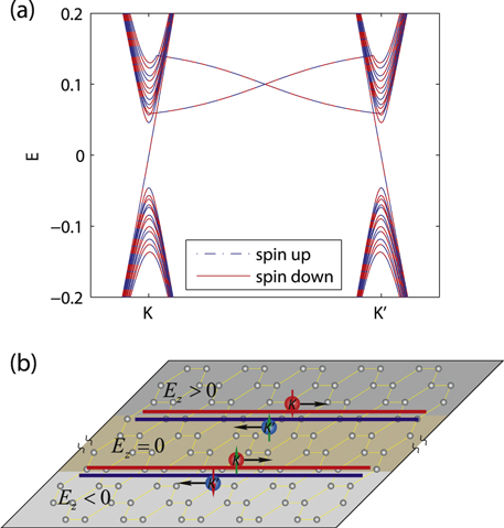
Figure 6. Band structure (a) of a silicene ribbon with two interfaces (b) created by  ,
,  and
and  . The spin-up and spin-down bands are overlapped in (a) and two helical TIS form and sustain the spin–valley-dependent currents in (b).
  ,
,  ,
,  and other parameters are given in text.
Download figure:
Standard image High-resolution imageIt is expected that the dissipationless spin–valley-dependent currents in the TIS are protected by both spin-conservation and valley-conservation in comparison to pure valley current or pure spin current, i.e., it is immune to not only moderate nonmagnetic disorder (spin-independent scattering), but also long-range magnetic or nonmagnetic disorder (intravalley scattering). Although the K and  valleys are related to each other by time reversal symmetry like the spin counterpart, the valley is defined in the honeycomb lattice structure, so the nonhoneycomb lattice scattering will lead to mixing of the K and
  valleys, and moreover, the large-momentum transfer from the short-range disorder could also bring about the intervalley scattering.
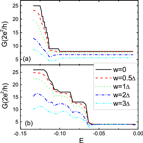
In figure 7, we calculate the short-ranged nonmagnetic disorder effect on the pure valley currents and spin–valley locked currents. The lattice on-site energy  is randomly taken in the range
 ![$\left[ -W,W \right]$](https://content.cld.iop.org/journals/1367-2630/16/4/045015/revision1/njp492003ieqn189.gif) and W is the disorder strength. In calculations, the lattice parameters are taken the same as those in figure 4(c), there is eight interface states constructed in the ribbon since
and W is the disorder strength. In calculations, the lattice parameters are taken the same as those in figure 4(c), there is eight interface states constructed in the ribbon since  . The length of the disorder region is set as
  , so the scattering-region size is estimated to be about 150 nm
  nm, and the disorder average is performed over 400 sample configurations. In figure 7(a) there is no SOI, the conductance platforms at
  readily collapse with a weak disorder, while the TIS conductance platform in the energy gap are robust in the weak disorder. Under a stronger disorder, the TIS conductances are severely reduced. This is because the short-ranged disorder can lead to the intervalley scattering. When the SOI is turned on in figure 7(b), it is seen that the TIS conductance platform in energy gap
  is fairly solid and can survive a much stronger disorder in comparison to those in figure 7(a). The reason is that the spin-conservation provides the extra protection to the TIS or the spin–valley-dependent currents.
Figure 7. Conductance versus Fermi energy E for different short-ranged disorder strengths W without SOI  in (a) and with SOI
  in (b). Parameters are
  and
and  .
.
Download figure:
Standard image High-resolution image
5. Conclusion
In summary, we have investigated the multiple TIS in the bulk silicene created by a spatially alternative electric field. It was found that the reversal of the electric field direction so as to the staggered potential changes the valley Chern number, so the multiple TIS could be created in the energy gap opened by the SOI or the staggered potential. The TIS are contributed by the K and  electrons in contrast to the usual helical edge states contributed by the X point electrons, and they sustain dissipationless valley currents or spin–valley-dependent currents, which are immune to both the intravalley and nonmagnetic scattering. The coupling among the multiple TIS may lead to an excitation gap that depends on the even or odd number of the interfaces created in the bulk silecene. Our results may shed light on engineering topologically-protected conductive channels in the bulk of an insulator.
Acknowledgments
The work was supported by the General Research Fund of the Research Grants Council of Hong Kong SAR, China (Project No. CityU 100311/11P). We are also grateful for support from NSFC (11274059 and 11274260) and NSF of Jiangsu Province (BK20131284).