


Abstract
We demonstrate sub-cycle manipulation of mid-infrared optical waveforms in the time domain. This goal is accomplished via efficient reflection at a semiconductor surface induced by femtosecond interband excitation. The ultrafast response of this process allows slicing of high-field multi-terahertz transients down to the single optical cycle. Ultrabroadband and phase-stable transients with peak amplitudes beyond 10 MV cm−1 are obtained, paving the way for efficient coherent control of light–matter interaction in the non-perturbative regime. The microscopic analysis of electron–hole plasma generation in germanium reveals a decisive role of two-photon absorption allowing efficient slicing up to mid-infrared frequencies.
Export citation and abstract BibTeX RIS

Content from this work may be used under the terms of the Creative Commons Attribution 3.0 licence. Any further distribution of this work must maintain attribution to the author(s) and the title of the work, journal citation and DOI.
1. Introduction
Recent efforts in ultrafast science are increasingly pointing towards the achievement of full optical control of fundamental physical processes. This goal motivates development of techniques for tailoring electromagnetic transients with temporal precision better than an optical cycle. Typically, this task is achieved by extending the spectral bandwidth of a pulse to more than an octave or by coherent synthesis of broadband sources [1–3]. Other existing methods for femtosecond optical pulse shaping in the visible and near-infrared spectral range mostly rely on intensity and phase control performed in the frequency domain [4]. However, such an approach does not enhance spectral bandwidth and imposes technical limitations when extended to mid- and far-infrared regions. Nevertheless, intense pulses in these spectral regions are especially appealing as they enable control of low-energy fundamental excitations in condensed matter [5, 6], and observation of previously elusive transport phenomena in high electric fields [7–9]. Phase-stable terahertz transients used for these investigations are typically generated via second-order nonlinear processes like, e.g., optical rectification [10] or difference frequency generation (DFG) [11]. Control of the envelope shape of such waveforms may be achieved by varying either the intensity profile [12–14], or the polarization state [15] of the driving pulses, or by employing periodically poled nonlinear crystals with specially designed domain structures [16].
Here, we introduce an alternative approach to tailor multi-terahertz (multi-THz) transients directly in the time domain by means of an ultrafast semiconductor mirror. This device is switched into the reflecting state by a near-infrared control pulse, allowing precise slicing of phase-stable mid- and far-infrared wave packets on sub-cycle timescales. In contrast to manipulation in the frequency domain, this method inherently increases the bandwidth by generation of new spectral components. An optical switch based on a semiconducting mirror was first employed for shortening nanosecond pulses from CO2 lasers down to sub-picosecond durations [17]. Naturally, such a dramatic reduction of the pulse duration renders the conversion process inefficient and limits the approach to operating on the envelope rather than directly on the electric field. Here, we show for the first time sub-cycle slicing of optical waveforms, relying on intense and phase-locked few-cycle transients [11, 18, 19]. As an example, this technique provides a single-optical-cycle multi-THz pulse with a peak electric field exceeding 10 MV cm−1. The impact of the slicing process on the electric field is captured directly in the time domain with the technique of ultrabroadband electro-optic sampling (EOS) [20, 21].
2. Demonstration of sub-cycle switching
Figure 1 shows a sketch of the experimental setup and the concept of the ultrafast switching mirror. A broadband transient centred at 23.7 THz with pulse energy of 2 μJ is obtained by DFG between two near-infrared pulses in a 1050 μm thick gallium selenide (GaSe) emitter crystal [18]. These multi-THz waveforms are focused by an off-axis parabolic mirror onto a germanium (Ge) wafer which serves as a switching element. The main advantages of Ge are the absence of polar phonons leading to vanishing Reststrahlen dispersion and negligible absorption in the mid- and far-infrared combined with low effective electron mass. The intrinsic Ge wafer has a thickness of 500 μm and a resistivity larger than 45 Ω cm. In the unperturbed state the semiconductor is fully transparent to the multi-THz radiation incident at Brewster's angle (αB,Ge ≈ 76°) and the reflected multi-THz field is negligible. Ultrafast switching into a highly reflective state is achieved by photoexcitation with a femtosecond control pulse that generates a high density N of electron–hole pairs via direct interband absorption (figure 1(b)). The resulting plasma acts as a mirror if N is large enough to screen the incoming field. To this end, the effective plasma frequency νp has to exceed the spectral content of the THz pulse. The Drude model gives an expression for the mid-infrared dielectric function of the photoexcited Ge wafer at frequency ν:
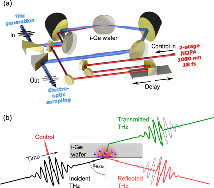
Figure 1. (a) Phase-locked linearly-polarized multi-THz radiation (blue) is focused onto an ultrafast semiconductor switch (intrinsic Ge wafer) by an off-axis parabolic mirror. The reflected THz waveform is collimated with a second parabolic mirror and detected by electro-optic sampling. Ultrashort near-infrared NOPA control pulses (red) trigger the reflectivity onset of the semiconductor switch. (b) Mid-infrared is completely transmitted under incidence on the unexcited Ge wafer at Brewster's angle. A dense electron–hole plasma generated by the control pulse in the semiconductor causes high-contrast switching into a reflecting state within a time interval shorter than a cycle of the multi-THz field. This step-like switching ensures that optical cycles preceding the control pulse are transmitted, while the following ones are reflected, thus slicing the total waveform into two channels.
Download figure:
Standard image High-resolution imageHere  is the dielectric constant of Ge in the absence of plasma, γ is the scattering rate and νp
the plasma frequency. The latter parameter depends on the density and the reduced effective mass (μeff) of the electron–hole pairs as
is the dielectric constant of Ge in the absence of plasma, γ is the scattering rate and νp
the plasma frequency. The latter parameter depends on the density and the reduced effective mass (μeff) of the electron–hole pairs as
where q is the elementary charge and  the vacuum permittivity. For an underdamped plasma (γ ≪ νp
) the dielectric function ε (ν) becomes negative in the case of ν < νp
leading to a strong enhancement of the Ge reflectance. Thus, femtosecond control pulses of relatively high energy and with duration shorter than the THz optical cycle are required for efficient slicing.
the vacuum permittivity. For an underdamped plasma (γ ≪ νp
) the dielectric function ε (ν) becomes negative in the case of ν < νp
leading to a strong enhancement of the Ge reflectance. Thus, femtosecond control pulses of relatively high energy and with duration shorter than the THz optical cycle are required for efficient slicing.
We generate 18 fs short control pulses with energies up to 15 μJ centred at a wavelength of 1080 nm using a two-stage non-collinear optical parametric amplifier (NOPA) [22]. The setup is aligned to achieve optimal spatio-temporal overlap and wavefront matching between control pulse and multi-THz transient which are mandatory requirements for high contrast sub-cycle switching. The confocal beam waist of the multi-THz transient at the ultrafast semiconductor switch is approximately 130 μm. The spot size of the control pulse is matched to the size of the mid-infrared focus. A precise control of the slicing process is obtained by varying the temporal delay t2 of the excitation pulse with respect to the mid-infrared transient using a delay stage. A weak residual reflection signal (4% of incident intensity) in absence of the switching pulse is observed due to slight deviations from Brewster's angle caused by the focusing of the multi-THz beam. The train of control pulses is modulated by a mechanical chopper, allowing us to discriminate the background signal and to subtract it from the detected waveforms. The reflected transient is collimated with a second off-axis parabolic mirror. The progress in cycle-by-cycle slicing is monitored directly in the time domain using EOS with a 10 μm thick (110)-oriented zinc telluride (ZnTe) sensor on a (100) ZnTe substrate [21].
Figure 2 depicts time-domain profiles of the electric field of sliced multi-THz waveforms and their amplitude spectra. The fluence of the control pulse is set to 13.7 mJ cm−2. If the control pulse precedes the broadband transient (t2 ≈ −150 fs), we observe a reflection of the complete waveform with a duration of 104 fs containing 2.5 oscillation cycles of the electromagnetic field (figure 2, dashed lines in left panels). The corresponding amplitude spectrum (figure 2, dashed lines in right panels) is centred at 23.7 THz with a bandwidth of 5.9 THz (FWHM). By adjusting the time of plasma generation t2, we are able to control the temporal position of the reflectivity onset and hence to slice the THz transient with sub-cycle precision. This process is illustrated in figures 2(a)–(c) where the reflected waveforms and their spectra are shown by solid lines for three different delay times t2. The waveform is progressively sliced to pulse durations of 86 fs (2.0 optical cycles), 75 fs (1.7 optical cycles) and 50 fs (1.1 optical cycles), respectively. In the right panel of figure 2, one can clearly see the simultaneous generation of new frequency components in the wings of the spectrum. In fact, time-domain switching affects the frequency content of the THz pulse, resulting ultimately in a doubling of spectral bandwidth for the single-cycle case (figure 2(c)). This result is a frequency-domain manifestation of the temporal amplitude modulation caused by the ultrafast action on a sub-cycle timescale. Consequently, the manipulation of intense pulses allows us to generate single-cycle THz transients while preserving 10 MV cm−1 peak electric fields.

Figure 2. (a)–(c) Real time profiles of the electric field of multi-THz transients (left panels) and corresponding amplitude spectra (right panels). The dashed line represents the fully reflected waveform. Adjustment of the delay time t2 between control pulse with a high fluence of 13.7 mJ cm−2 and the reference transient modifies the pulse duration of the transient with sub-cycle precision. The solid lines illustrate sliced THz waveforms and corresponding spectra at (a) t2 = −69 fs, (b) t2 = −24 fs and (c) t2 = 12 fs, respectively.
Download figure:
Standard image High-resolution image3. Mechanism of ultrafast switching in Ge
The sub-cycle slicing demonstrated in the previous section relies strongly on the switching time of the ultrafast mirror. To assess this performance, we investigate the onset of reflectivity by tracing the field of the multi-THz waveform as a function of delay t2 at a fixed EOS time t1. Figure 3 shows the evolution of the reflected field at the maximum (circles) and the adjacent minimum (squares) of the reference waveform. In the case of an instantaneous plasma response, the onset time is limited by the time-integrated control pulse convolved with the instrument response function of our electro-optic detection scheme [21]. Interestingly, the switching dynamics exhibits distinct differences depending on the excitation density. In case of a moderate fluence of 1.9 mJ cm−2 (figure 3(a)), the rise time of the reflected multi-THz field amounts to 110 fs. It is considerably longer as compared to the limit imposed by the duration of the control pulse and the bandwidth of the 140 μm thick GaSe electro-optic detector used in this case. This finding may be understood by considering that the density of photo-generated carriers N limits the reflectivity bandwidth of the plasma switch to νp , leading to a response time of approximately 1/νp . Furthermore, we observe that the initial rise of the reflectivity is followed by a pronounced decrease on a sub-100 fs timescale. This effect must be due to significant changes in the electronic distribution in photoexcited Ge which affect νp (see equation (1) and discussion below). In stark contrast, the control pulse with a high fluence of 13.7 mJ cm−2 leads to a step-like build-up of reflectivity within 45 fs without a subsequent drop (figure 3(b)). This switching time is now close to the response function expected from the finite duration of the pump pulse and the total bandwidth of the electro-optic detection scheme (see dashed line in figure 3(b)). Specifically, it is shorter than the period of the oscillation period of the multi-THz field, ultimately enabling the sub-cycle slicing achieved in our experiment.

Figure 3. Electric field for a fixed electro-optical sampling time t1 as a function of the time of plasma generation t2. The evolution of the reflected field maximum (circles) and the adjacent minimum (squares) is shown for different control fluences: (a) moderate fluence of 1.9 mJ cm−2 and (b) strong fluence of 13.7 mJ cm−2 (note change in abscissa scale). Fitting curves (solid lines) correspond to onset times of 110 fs and 45 fs for panels (a) and (b), respectively. Dashed lines represent the simulated reflectivity onset of an ideal optical switch (infinite bandwidth) limited only by the duration of the control pulse and the response function of the electro-optic detector.
Download figure:
Standard image High-resolution imageTo gain quantitative understanding of the underlying switching mechanisms we consider the electronic and optical properties of intrinsic Ge in closer detail. Figure 4(a) depicts the relevant part of the band structure with a direct gap at the Γ-point equal to 805 meV at room temperature [23]. Therefore, linear excitation with the near-infrared control pulse (hνc = 1.1 eV) promotes electrons into the Γ-valley with residual excess energy. Note that indirect linear excitation of electrons into the L-valley is negligible because this process needs to be assisted by a phonon in order to conserve momentum. However, photoexcited electrons at the bottom of the Γ-valley get transferred into the L-valley within approximately 230 fs by scattering with phonons via the deformation potential [24, 25]. Excitation occurs far above the Γ-minimum in our case and the excitation density is high enough to support significant carrier–carrier scattering, resulting in a shorter intervalley transfer time of less than 100 fs. As the isotropic average of the electron effective mass in the L-valley (meff,L
= 0.12 m0) is higher than the one in the central minimum (meff,Γ
= 0.04 m0) [26], intervalley scattering should lead to reduction of the plasma frequency by a factor of approximately  , according to equation (1). The described scenario fully explains the features in the dynamics (figure 3(a)) if the starting νp
is comparable to the centre frequency of a transient. Nevertheless, considering only single-photon absorption (1PA) at a fluence of 1.9 mJ cm−2, we would expect a plasma frequency in excess of 100 THz (figure 4(b)), providing a fast switch without the overshoot behaviour. However, only a limited density of states may be accessed by single-photon direct transitions: for moderate fluences, our estimate (figure 4(b)) predicts saturation of νp
to values around 30 THz due to Pauli blocking of interband transitions. Assuming a spectral width of the control pulse of 26 THz as well as parabolic bands, the saturation density of 1PA is estimated to nSat ≈ 5 × 1018 cm−3 as shown in figure 5(a). The saturation fluence is defined by
, according to equation (1). The described scenario fully explains the features in the dynamics (figure 3(a)) if the starting νp
is comparable to the centre frequency of a transient. Nevertheless, considering only single-photon absorption (1PA) at a fluence of 1.9 mJ cm−2, we would expect a plasma frequency in excess of 100 THz (figure 4(b)), providing a fast switch without the overshoot behaviour. However, only a limited density of states may be accessed by single-photon direct transitions: for moderate fluences, our estimate (figure 4(b)) predicts saturation of νp
to values around 30 THz due to Pauli blocking of interband transitions. Assuming a spectral width of the control pulse of 26 THz as well as parabolic bands, the saturation density of 1PA is estimated to nSat ≈ 5 × 1018 cm−3 as shown in figure 5(a). The saturation fluence is defined by

where α = 5 × 104 cm−1 is the linear absorption coefficient at the frequency of the control pulse [27]. Assuming negligible energy relaxation during the pump pulse, the density of charge carriers generated by 1PA with saturation can be estimated by

where Φc is the fluence of the control pulse.
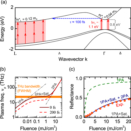
Figure 4. (a) Band structure of Ge: single-photon absorption (1PA) of control pulse (hνc = 1.1 eV) is depicted by single vertical arrows, while two-photon absorption (2PA) is indicated by double arrows. The dashed arrow denotes intervalley scattering. (b) Plasma frequency νp as a function of pump fluence calculated taking into account 1PA with saturation and 2PA effects directly after excitation (solid line) and after 200 fs, when the majority of photoexcited electrons have scattered from the Γ- to the L-valleys (dashed). The filled area marks the spectral content of the phase-locked transient at a carrier frequency of 23.7 THz. The dash-dotted lines denote the asymptotic cases of pure 1PA and 2PA. (c) Reflectance of the ultrafast semiconductor switch as a function of pump fluence: experimental data (circles) are shown versus theoretical estimates calculated for different absorption channels for unsaturated 1PA (dashed), 1PA with saturation (dash-dotted) as well as 1PA with saturation and 2PA (solid line) cases.
Download figure:
Standard image High-resolution image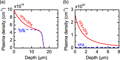
Figure 5. Calculated density of excited charge carriers as a function of the penetration depth generated by saturated 1PA and 2PA (solid line) and solely by saturated 1PA in the Γ-valley of Ge (dashed line). The control pulse fluence is selected in accordance to the experimental data sets depicted in figure 3: (a) 1.9 mJ cm−2 and (b) 13.7 mJ cm−2. Note the difference in the scaling of both axes.
Download figure:
Standard image High-resolution image
For higher fluences, however, two-photon absorption (2PA) allows direct access to excitation pathways in the L-valley where much larger joint densities of states are available owing to nearly parallel alignment of conduction and valence bands (figure 4(a)).
Figure 5 shows the profiles of plasma density near the Ge surface calculated for the same excitation fluences as in figure 3. For a moderate control pulse fluence of 1.9 mJ cm−2, a carrier density of 1 × 1019 cm−3 is estimated near the surface. This value already exceeds the saturation density nSat by a factor of 2. As can be seen from the comparison with the 1PA case, 2PA dominates near the surface of the semiconductor switch, where the pump intensity is highest, leading to an enhanced density of the electron–hole plasma. A strong control pulse fluence of 13.7 mJ cm−2 results in a remarkable enhancement and the plasma density reaches 2.5 × 1020 cm−3 (see figure 5(b)). Thus, the 2PA channel allows us to obtain a much higher plasma frequency when the excitation fluence exceeds a value of 5 mJ cm−2. In this regime, the majority of excitation occurs directly to the L-valley and intervalley scattering becomes irrelevant (figure 4(b)). As a consequence, the reflectivity shows a step-like onset without a transient overshoot as shown in figure 3(b). A plasma frequency of νp ≈ 100 THz now supports high reflectivity for the full THz bandwidth.
Our results attest that strong optical excitation of Ge in the regime of 2PA is indispensable for efficient sub-cycle slicing of multi-THz transients. The fact that 2PA plays a key role in the generation of a dense electron–hole plasma in Ge is quantitatively demonstrated by a measurement of fluence-dependent reflectance. Figure 4(c) shows experimental data (circles) obtained for excitation fluences between 1 mJ cm−2 and 20.5 mJ cm−2. Theoretical reflectance is calculated for different absorption scenarios: (i) unsaturated 1PA (dashed line), (ii) 1PA with saturation (dash-dotted line) and (iii) 1PA with saturation and 2PA (solid line). The 2PA coefficient (β = 5.5 cm GW−1) is implemented according to the literature [28, 29]. The reflectivity for p-polarized light is calculated for a layered system consisting of vacuum (n = 1), homogeneously excited Ge with electron–hole plasma containing Γ- and L-valley electrons (n =  , see equation (1)) and an intrinsic Ge background (nGe = 4). To model the reflectivity, we considered the effective density of the plasma with respect to the depth profile of photoexcitation [30]. For saturated one-photon absorption, the excitation depth extends beyond 10 μm (figure 5(a)). After the onset of 2PA the plasma density becomes significantly higher closer to the surface (figure 5(b)). Nevertheless, the thickness of the plasma layer well exceeds the penetration depth for 24 THz radiation (380 nm), supporting efficient reflection of the transients. The best agreement of our simulation with the experimental data was obtained for a transient damping rate γ = 40 THz. It is clearly seen that an adequate description of the experimental findings can be achieved only by taking into account saturation of linear absorption and two-photon excitation. Considering the maximum reflectivity of 50% and the residual background from the unexcited Ge wafer of 4% we obtain a modulation efficiency of 85% for the intensity.
4. Conclusion
Time-domain slicing based on an ultrafast semiconductor mirror enables control of ultrashort optical waveforms on a sub-cycle timescale. With this technique, we succeed in synthesis of a single oscillation of light at mid-infrared frequencies and with a peak electric field above 10 MV cm−1. New spectral components are generated by ultrafast modulation of the carrier field. This result demonstrates high potential for direct pulse shaping in the time domain paving the way to generating single-cycle transients beyond 100 MV cm−1 [18]. Furthermore, the modulation bandwidth can potentially be doubled by scaling up the power of the few-femtosecond near-infrared switching pulses. In addition, the study unveils the importance of 2PA in order to achieve high plasma frequencies approaching the near infrared. Experiments on extremely nonlinear light–matter interaction and sub-cycle optical biasing are the natural application for the pulses tailored by our slicing technique.
Acknowledgements
Financial support by Advanced Grant 'UltraPhase' of the European Research Council (ERC-2011-AdG No. 290876) and by DFG via SFB767 is gratefully acknowledged.