


Abstract
Chalcogenide-based phase-change materials play a prominent role in information technology. In spite of decades of research, the details of electrical transport in these materials are still debated. In this article, we present a unified model based on multiple-trapping transport together with 3D Poole–Frenkel emission from a two-center Coulomb potential. With this model, we are able to explain electrical transport both in as-deposited phase-change material thin films, similar to experimental conditions in early work dating back to the 1970s, and in melt-quenched phase-change materials in nanometer-scale phase-change memory devices typically used in recent studies. Experimental measurements on two widely different device platforms show remarkable agreement with the proposed mechanism over a wide range of temperatures and electric fields. In addition, the proposed model is able to seamlessly capture the temporal evolution of the transport properties of the melt-quenched phase upon structural relaxation.
Export citation and abstract BibTeX RIS

Content from this work may be used under the terms of the Creative Commons Attribution 3.0 licence. Any further distribution of this work must maintain attribution to the author(s) and the title of the work, journal citation and DOI.
1. Introduction
Chalcogenide-based phase-change materials play a key role in the next-generation memory and computing technologies [1–3]. Compounds such as GeTe can be rapidly and reversibly switched between the amorphous and crystalline states [4]. This is accompanied by a significant change of their optical and electrical properties. Devices such as phase-change memory (PCM) cells rely on the orders of magnitude difference in resistivity between the two phases to store information. A detailed understanding of electrical transport in these materials, especially in the more resistive amorphous phase, is important for the design of such devices. Moreover, the amorphous phase created via glass transition is in an unstable state and undergoes structural relaxation or 'drift' as the latter is commonly referred to. This manifests as a continuous temporal evolution of the transport properties. The resistivity of the amorphous phase is strongly field dependent. At high fields, the amorphous phase abruptly switches to high conductivity upon the so-called threshold switching which is thought to be purely an electronic phenomenon [5, 6]. In this article we aim to study the electronic transport prior to threshold switching. This regime commonly referred to as the sub-threshold regime (low to intermediate field range) has significant technological relevance because it is crucial for deciphering the stored information in memory and synaptronic applications, and hence continues to be an active area of research [7].
In disordered materials, electrical transport occurs either via localized states through quantum-mechanical tunneling or via extended states dominated by trapping and release events (multiple-trapping) [8]. In several amorphous phase-change materials, it has been shown that multiple-trapping can successfully describe the low field conductivity measurements at temperatures above approx. 200 K, whereas at lower temperatures tunneling in localized states dominates transport [9, 10].
To explain the variation of conductivity with the electric field in the multiple-trapping picture for disordered materials, the Poole–Frenkel effect is commonly used [11–13]. The Poole–Frenkel model is based on thermal emission from ionizable defect centers that are assumed to create a Coulomb potential. The ionization energy is then lowered upon the electric field by  with
with

where F is the applied electric field, e the electronic charge,  0 the vacuum permittivity and r the relative high-frequency (HF) dielectric constant. The conductivity is expected to follow a law (Poole–Frenkel) of the form
 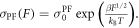 When the defect centers are close to each other so that there is significant overlap between the Coulomb potentials, it has been shown by using a two-center Coulomb potential that the ionization energy lowering upon field is
  [13]. The conductivity is then expected to follow a law (Poole) of the form
 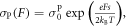 where s is the distance between the two centers.
Most of the early work on field dependence of conductivity in phase-change materials focussed on as-deposited thin films and Poole–Frenkel type transport was typically observed at high fields [14, 15]. One of the first studies of electrical transport in nanoscale PCM devices was by Ielmini and Zhang where they mostly observed an ohmic regime at low fields and Poole-type behavior at higher fields [16]. However, experimental measurements since then clearly showed the existence of three distinct regimes, an ohmic regime, a Poole regime and a Poole–Frenkel regime [17, 18]. The ohmic regime occurs at very low fields and the transition from Poole to Poole–Frenkel conduction occurs at high fields [19]. Moreover, the point at which this transition occurs may vary upon structural relaxation [20].
In the past, this transition from Poole to Poole–Frenkel conduction had also been investigated in the general context of disordered materials. In one approach, proposed by Ieda et al, a state of energy δ below the conduction band was introduced in which the electrons are considered as free carriers [21]. Recently, this approach was applied by Beneventi et al to phase-change materials [19]. The resulting derivation gives a simple analytical description in which the transition from Poole to Poole–Frenkel conduction can be tuned by adjusting the parameter δ, however at the cost of a rather unclear physical picture. Yet another model by Pillonnet et al showed that the Poole to Poole–Frenkel transition could also be deduced from Hill's approach [13] by considering a carrier in a pair of Coulombic wells separated by a distance s [22]. Hill's model, however, assumes, just like Ielmini and Zhang, immediate re-trapping after emission which leads to a constant travel distance of the charge carriers.
The key idea behind our modeling approach is to adhere to the original multiple-trapping picture, in which the conductivity is calculated based on the transport of carriers via free states, without limiting the free travel distance to the nearest-neighbor distance as explained in detail in section 2. The field dependence of the free carrier density is then captured via 3D Poole–Frenkel emission of carriers from a two-center Coulomb potential. We demonstrate that this model is sophisticated enough to capture the subthreshold transport properties of amorphous-as-deposited phase-change materials in thin films (similar to the experimental conditions in early work on amorphous chalcogenides) as well as of melt-quenched phase-change materials in nanometer-scale memory devices as typically used in recent studies. First, the model is validated over a wide temperature range on as-deposited GeTe line cells on the micrometer scale. Then, we show that the model can also capture the transport behavior of the same material, but melt-quenched, in a nanoscale PCM cell with similar physical parameters. Finally, we show how the model can capture the evolution of the transport properties of the melt-quenched phase upon structural relaxation. The ability to describe the transport properties over such wide range of experimental conditions convincingly demonstrates the efficacy of our modeling approach. In addition, we provide some insights into the microscopic picture of the transport mechanism based on the experimental results and fit parameters.
2. Modeling
To develop the transport model, we first study the emission of carriers from the Coulombic centers to free states under the influence of a uniform applied field, F. For electrons, assuming Boltzmann statistics, the density of free carriers under an applied field n(F) can be calculated as

where θ is defined as the angle between the electric field and the direction of escape, K is a constant, Ea the activation energy and EPF(F, θ) the energy barrier lowering due to the Poole–Frenkel effect. Note that we consider emission into a complete sphere [12, 21, 23]. As we will show later, this approach is needed to describe the experimentally observed ohmic behavior at low fields, which would not be possible by considering emission strictly along the field direction.
To calculate the barrier lowering EPF(F, θ), the following potential profile is considered :

In this potential, the electron is under the influence of an applied field F and of Coulombic wells situated at r = 0 as well as at r = s in all directions. The θ-dependence of the potential allows including all possible escape scenarios in a disordered solid considering interaction between only two sites. Note that the two sites considered do not need to necessarily coincide in energy, but are assumed to be sufficiently deep in the gap so that they do not get delocalized by the application of the electric field. As motivated in the next paragraphs, the choice of considering only two sites was made in order to reflect a critical transition within the transport path of the amorphous system that will dominate the resistivity. The energy barrier lowering is then calculated as

Note that the term  in equation (3) is included so that
  This way, Ea in equation (2) can be taken as the experimentally measured activation energy. The latter was assumed to vary with the temperature, because of the measured temperature dependence of the optical bandgap, as
  with ξ = 0.5 × 10⁻⁶ eV K−2 [10, 24]. Figure 1 shows the potential (equation (3)) along the directions θ = 0 and θ = π as well as the corresponding energy barrier lowering.

Figure 1. Schematic illustration of the transport model. The potential profile given by equation (3) is used to calculate the Poole–Frenkel energy barrier lowering in the directions θ = 0 and θ = π (left plot). The blue dotted lines are the single potential wells without any applied field. The applied field F reduces the potential barrier in the direction θ = 0 and increases it along θ = π. After emission, the carrier travels in free states, experiencing some scattering, until it gets re-trapped after a time τt which is assumed to be field-independent (right plot). The distance d traveled by the free carrier, which is the product of the velocity and the free lifetime, is therefore field-dependent according to the mobility model (equation (5)).
Download figure:
Standard image High-resolution imageThe energy Ea is thus the energy for activation over the top of the Coulombic barrier at F = 0, and is used as the energy reference for activation to free states. The carriers emitted this way are assumed to be free in the sense that they can be accelerated by the electric field with a certain mobility μ over sufficiently large distances, eventually larger than s. This assumption is justified in phase-change materials where Ea is found to be close to half of the optical bandgap [15]. Therefore, the carriers emitted over the top of the Coulombic barrier are more subject to band rather than hopping transport [7].
Additionally, it is worth pointing out that we do not view transport as occurring through a chain of centers spaced by the same s. This clearly cannot be realistic for a disordered system which is in essence characterized by a distribution of random site energies and inter-site distances. We instead believe that the resistor network idea in which the highest resistance in the percolation cluster is the dominating process [25] is more appropriate to describe this type of transport. The transport path in our model will be the least resistance continuous path through the system composed of multiple trap-and-release events to free states. Since the sites within the transport path are randomly distributed with different trap and release parameters, there will be a critical transition that will dominate the resistivity which can be associated to an inter-site distance s and an activation energy Ea. We therefore collapse multiple transitions that certainly will occur into a single average (or rather dominating and therefore relevant) event, and it is this single event that is described by equations (2), (3) and (4).
After emission, the carrier travels in free states, experiencing some scattering, until it gets re-trapped after a certain time. The conductivity can then be calculated for a free mobility μ by 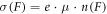 and the current density by
  However, in amorphous materials, there is a disagreement in the research community on whether the free mobility should be considered field-independent [26] or rather the free carrier velocity should be independent of the field (therefore
  ) [14, 27]. However, it is generally admitted that the free lifetime of the released carriers is field-independent [8, 12]. A constant free mobility therefore means that the carrier would drift for a constant time before being re-trapped, but without any limitation on the distance traveled (trap-limited band transport). This approach in particular leads to Ohm's law if the amount of released carriers does not depend on the field.
Conversely, if a constant free carrier velocity is assumed, it means that not only the lifetime of the free carrier is constant but also the distance that it travels before being re-trapped. If this distance is defined as the distance s as is commonly done [13, 16], transport can be viewed as trap-and-release events between the Coulombic traps. For high fields, this assumption leads to good agreement with experimental data on phase-change materials as well as on amorphous oxides [23]. However, this picture cannot describe the ohmic behavior observed at low fields. Therefore, a common approach has been to subtract the currents in and against the field direction [16] to recover Ohm's law. This, however, is incompatible with the multiple-trapping model. Indeed, if carriers are emitted to free states, they should participate equally to the conduction regardless of the direction of escape. This is why the emission contributions in equation (2) are linearly summed and not subtracted when the direction of escape is against the field.
As a compromise between the two approaches, i.e. to achieve trap-limited band transport at low fields but also allow for a constant travel distance to occur at high fields, we expressed the free mobility in a more generic way as [28, 29]

where vsat is a saturation velocity and μ0 the low-field mobility. The saturation field  was then set to a value that best described our experimental data.
The model presented above leads to three distinct regions in the transport behavior depending on the applied field: (i) ohmic regime (very low field,  ), (ii) Poole regime (low field,
  ) and (iii) Poole–Frenkel regime (high field,
  ). A typical measure of the transition field Ft between the Poole and Poole–Frenkel regimes is [22]

For F < Ft, 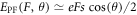 and
and  which is equivalent to the standard Poole conduction models derived elsewhere [13, 16]. We also define the transition field FO between the ohmic and Poole regimes as the field at which the second term of the Taylor expansion of the sinh function is 10% of the first term, i.e.,

3. Results
Next, we will present the experimental results that test the validity of the proposed model in describing the transport properties over a wide range of experimental conditions. As mentioned earlier, most of the early work on amorphous chalcogenides has been on as-deposited (typically via physical vapor deposition) thin films. However, in current phase-change devices, the amorphous phase is created via the melt-quench process where the cooling rate is a staggering 1011 K s−1 [30]. Moreover, in these devices, we can probe the transport properties down to tens of nanometers. To bridge these two worlds as well as to verify the transport model in a wide range of experimental conditions, we experimented on two different device platforms
The line cells were fabricated with as-deposited phase-change materials using optical lithography techniques on silicon substrate with 100 nm thermally grown silicon dioxide. The electrodes consisted of an adhesion layer of titanium (10 nm) and 120 nm of tungsten in contact to the phase-change material. The phase-change material was GeTe with Ge content around 51%–54% cross-checked using Rutherford backscattering. The phase-change deposition was done using dc magnetron sputtering in high-purity Argon atmosphere at 20 W. The nominal distance between electrodes was 2 μm and the contact area 100 nm×20 μm. The distance between the electrodes and the width of the phase-change film were checked with SEM measurements. The vertical film thickness (100 nm) was calculated from the calibrated sputter rate. The error on the vertical thickness determination is expected to be less than 5%. A schematic illustration is shown in figure 2.

Figure 2. Experimental results on micrometer-scale line cells. Resistance versus voltage characteristics of as-deposited GeTe line cells along with the proposed model (black lines) from 300 K down to 220 K.
Download figure:
Standard image High-resolution imageThe melt-quenched phase-change materials were studied using PCM mushroom-type cells fabricated in the 90 nm technology node with the bottom electrode created via a sub-lithographic key-hole process [31]. The bottom electrode has a radius of approximately 20 nm and the phase-change material has a thickness of 100 nm extending to the top electrode. The electrode material is TiN. The phase-change material is in the crystalline phase prior to experimentation. By applying current (denoted RESET current) pulses with nanosecond-scale trailing edges, it is possible to create amorphous regions on the length scale of tens of nanometers through the melt-quench process (see figure 3). The higher the amplitude of the RESET current, the larger is the amorphous region that is created. In such a serial configuration, electrical transport is dominated by the amorphous phase.

Figure 3. Experimental results on nanoscale PCM cells. Resistance versus voltage characteristics of GeTe PCM cells along with the proposed model. Also shown is the comparison with the standard Poole–Frenkel models found in the literature. Both the 3D Poole and 3D Poole–Frenkel models [13] fail to fit the entire R–V characteristics, whereas the agreement of the proposed model is excellent in the entire range of applied voltages.
Download figure:
Standard image High-resolution imageA JANIS ST-500-2-UHT cryogenic probing station that operates from 77 K to 400 K and offers a temperature stability of <50 mK was used for the electrical measurements. The cryostat is cooled with liquid nitrogen as cryogen. The temperature is measured at four points inside the chamber by calibrated Lakeshore Si DT-670B-CU-HT diodes with an accuracy of <0.5 K. Temperature regulation was done using a Lakeshore 336 Automatic Temperature Controller. Low-frequency probe tips were used for the electrical measurements on the line cells and a HF Cascade Microtech Dual-Z probe for the PCM cells. A Keithley 2612A SMU was used for dc voltage outputs and for measuring the corresponding current at the sample. The current resolution of the electrical setup is ∼1 pA.
In figures 2 and 3, we show the R–V (resistance versus voltage) curves recorded on the two device platforms and their fits to the proposed transport model. We chose to plot the resistance versus the square root of voltage rather than the common I–V characteristic because in this way the ohmic behavior at low fields as well as the Poole–Frenkel behavior at high fields are visible as straight lines. For completeness, all the experimental data and corresponding fits to the transport model plotted as current versus voltage are displayed in supplementary figure 1, available at stacks.iop.org/njp/17/093035/mmedia. The values of the parameters that were used in the model for the different devices are listed in table 1. The relative permittivity was assumed to be time and temperature independent based on Fourier-transform infrared (FTIR) spectroscopy measurements done on as-deposited phase-change materials. Those show that the change in the HF dielectric constant in the time and temperature ranges used in our experiments is expected to be very small (<2%) [32].
Table 1.
Parameters used in the model for the fits of figures 2–
4. A critical field for velocity saturation of  Vμm−1 was used in equation (5). For the PCM cells, the contact area is defined by the effective bottom electrode radius rBE. Thickness denotes the effective amorphous thickness ua for the PCM cells which is close to the difference between the real amorphous thickness and the heater radius, and thus the shortest pathway of conduction through the amorphous halfdome. For the line cells, thickness denotes the gap between the electrodes.
| Contact area | Thickness | s | s−3 |

|
r |

|
|
|---|---|---|---|---|---|---|---|
| Device | (nm) | (nm) | (cm−3) | (eV) | (m−1 V−1 s−1) | ||
| As-deposited GeTe | 100 nm×20 μm | 2000 | 8.1 |

|
0.315 | 13 |

|
| Melt-quenched GeTe PCM | π · (20 nm)2 | 15 | 8.1 | 1.9 × 10¹⁸ | 0.24 | 13 | 5.5 × 10²¹ |
| d-GST PCM, 700 μA RESET, 2 min at 300 K | π · (20 nm)2 | 9.5 | 2.4 | 7.2 × 10¹⁹ | 0.225 | 10 | 1022 |
| d-GST PCM, 700 μA RESET, 15 h at 300 K | π · (22 nm)2 | 9.5 | 2.9 | 4.1 × 10¹⁹ | 0.25 | 10 | 1022 |
| d-GST PCM, 850 μA RESET, 15 h at 300 K | π · (19.5 nm)2 | 12.2 | 3.0 | 3.7 × 10¹⁹ | 0.26 | 10 | 1022 |
Figure 2 shows the R–V curves recorded on as-deposited GeTe line cells along with the proposed model. The relative permittivity r was set to the value of the HF dielectric constant measured by Shportko et al [33] using FTIR spectroscopy. The activation energy, Ea0, was obtained from the low-field resistance measurements at different temperatures, leaving only the product  and s as fit parameters. Those were obtained by fitting the room-temperature data to the model. With all parameters fixed in this way, the model is able to capture the experimental data from 300 K down to 220 K up to fields of 20 Vμm−1 with an inter-trap distance of
  All three conduction regimes are visible, even though the regime of Poole conduction is rather small. Towards low temperatures, the transition from ohmic to Poole regime shifts to lower fields, whereas the transition from Poole to Poole–Frenkel stays constant. At low temperatures, fewer thermally activated carriers are available and thus field-assisted emission is important already at lower fields. The slight discrepancies seen at high fields and low temperatures could be due to additional current possibly related to the threshold switching mechanism, as previously observed in the literature [14, 34].
Figure 3 shows the R–V curves obtained from the GeTe PCM cells with melt-quenched amorphous regions. To compare the experimental data with the proposed model, we assume that the applied electric field is F = V/ua, where V is the applied voltage on the cell and ua an effective amorphous thickness roughly equal to the smallest pathway of conduction through the amorphous region. Moreover, the device area used for the calculation of the current is assumed to be  where rBE is an effective bottom-electrode radius. It has been shown that introducing these two effective parameters allows the mushroom cell geometry to be well approximated by a cylindrical geometry of radius rBE with a uniform field applied over ua [35].
For both temperatures measured, it can be clearly seen that the standard Poole model can only fit the low-field region well, and the Poole–Frenkel model only the high-field region. Only a hybrid approach such as the proposed model can fit the entire R–V characteristics over the full range of applied voltage. It is also interesting that the model can capture the R–V characteristics of the nanoscale PCM cell with melt-quenched GeTe using the same value of the inter-trap distance s as for the as-deposited GeTe in the micrometer-scale device. The activation energy of the melt-quenched phase was found to be lower than for the as-deposited phase, which is expected given the different thermal history and the higher amount of crystalline nuclei in the melt-quenched phase [36].
To test the validity of the transport model on alternate phase-change materials and also to investigate the influence of structural relaxation on the transport properties, we used PCM cells with doped Ge2Sb2Te5 (d-GST) [30]. Figures 4(a) and (b) show the R–V curves from these PCM cells that have undergone thermal annealing at 300 K for 2 min and 15 h, respectively. The amorphous regions are created with an identical RESET current of 700 μA at 300 K, then annealed and measured down to 180 K. Figure 4(c) shows R–V curves obtained from a larger amorphous region created with a RESET current of 850 μA. The data was fitted to the model by using ua, rBE and s as fitting parameters for all temperatures collectively. The values of the other parameters that were fixed are given in table 1. The relative permittivity was assumed to be lower than that of pure GST because of the doping [37].  was again extracted from the temperature dependence of the low-field data.

Figure 4. Influence of structural relaxation on transport properties. Measured resistance versus voltage characteristics of melt-quenched d-GST cells from 300 K down to 180 K for different annealing times and different RESET currents and the corresponding fits (black lines). An increase of the annealing time reduces the transition fields between the different conduction regimes and can be fully captured by an increase of the activation energy Ea0 and inter-trap distance s without any change in the resulting ua. As expected, a higher RESET current results in a higher ua, leaving the other parameters fairly constant.
Download figure:
Standard image High-resolution image
It can be seen that the model captures the transport behavior remarkably well in all cases. A slight increase in the fitting error with decreasing temperature (see figure 4(d)) can be interpreted as an increasing contribution of variable-range hopping to the electrical transport at lower temperatures [9], which is not taken into account in the present model.
Upon an increase of the annealing time from 2 min to 15 h, the transitions between the different conduction regimes shift to lower fields (figures 4(a) and (b)). The changes in the R–V characteristics can be fully captured by an increase of the activation energy  and of the inter-trap distance s, whereas the resulting ua did not change. The increase of activation energy upon structural relaxation is consistent with the experimentally observed increase in the optical bandgap [9, 10, 38]. The increase of s upon structural relaxation indicates that annealing of defects occurred, which would translate into an increase of the distance between the Coulombic centers [39]. It is truly remarkable that the seemingly intricate changes in the transport properties associated with structural relaxation can be captured by changing only the two parameters Ea0 and s. The fits of figure 4(c) also confirm that a higher RESET current mainly results in a larger ua, whereas the other parameters stay fairly constant.
4. Discussion
Even though the transport model developed here seems to capture well the variation of the conductivity with temperature and electric field above approx. 200 K, one could argue whether other bulk conduction mechanisms, such as hopping between localized states, may yield similar good agreement with the experimental data. Indeed, the field dependence of conductivity for hopping conduction as derived for example by Apsley et al [40] is rather similar to that obtained by Poole/Poole–Frenkel models typically derived in a multiple-trapping picture. Therefore, the field dependence of conductivity alone is not likely to give enough information to discriminate between one transport mode or the other. However, in amorphous phase-change materials, evidence for extended states conduction at high temperatures has been obtained in recent measurements of the density of states of GeTe via modulated photoconductivity [41] and simulations of the GeTe dark conductivity including hopping and multiple-trapping transport [9]. The optical bandgap of amorphous GeTe being around 0.8 eV [33], a measured activation energy of ∼0.3 eV for extended states conduction is explained by a shift of the Fermi level towards the valence band due to acceptor-like deep defects making the material p-type, in accordance with Seebeck measurements [41]. From these works, evidence is provided that conduction via localized states is dominating only below 200 K while at higher temperatures multiple-trapping transport dominates the low-field conductivity. The good agreement of the proposed transport model on a wide range of phase-change devices therefore seems to further support the evidence for multiple-trapping also at high-fields in amorphous phase-change materials.
Other conduction mechanisms that could perhaps explain our experimental data are Schottky emission and space-charge limited conduction. If a Schottky barrier would be present at the metal–amorphous junctions in our devices, a field dependence of the conductivity could arise from the modulation of this barrier with applied electric field [42]. However, if a Schottky barrier would dominate the conduction in the PCM mushroom cells, a rectifying diode-like I–V characteristic would be expected (see supplementary note 1). Since that is not observed in our devices (supplementary figure 2), it is thus reasonable to assume that the contact at the metal-amorphous junctions is fairly ohmic and that the observed field-dependence of conductivity comes mostly from the bulk amorphous material. In this case, the Poole–Frenkel effect is more appropriate to describe the electrical transport. Other evidence against Schottky emission in phase-change devices comes from early studies on GeTe thin films where it was observed that the I–V characteristics did not depend on the electrode material [15].
Regarding space-charge limited conduction, a distinctive feature predicted by this mechanism is a thickness dependence of the electrical transport properties [7, 34, 43, 44]. Early studies in the 1970s have shown that such dependence is generally not observed in thin films of chalcogenide glasses [34], and that seems to be the case for our devices as well (see supplementary note 2). Any field dependence of conductivity due to space-charge effects is thus apparently small compared to that of field-assisted trap-and-release. Additionally, we have shown in a parallel study that the conductivity of Ag4In3Sb66Te27 phase-change material line cells is independent of the device thickness ranging from 2 μm to 5 μm up to fields of 25 V μm−1 [45]. Other studies have shown reliably that the field at which phase-change materials switch to a high conductive state is independent of the device thickness ranging from 6 nm to 480 nm [46]. All those observations are inconsistent with a space-charge limited conduction mechanism.
In addition, we would like to add some remarks about the free mobility model (equation (5)) that we used. While the physical origin of a velocity saturation in amorphous materials is yet to be investigated, some arguments can be made based on the presented data to motivate the inclusion of such a model. If we would assume that the velocity saturation comes from optical phonon scattering as in crystalline materials, an estimate of the saturation velocity is given by  where Eph is the optical phonon energy and m* the effective mass in units of the electron mass me [29]. Mean phonon energies of about Eph = 15 meV have been measured by coherent phonon spectroscopy [47], Raman scattering [48] and calculated with density functional theory [49] in amorphous GeTe and GST. For the density of states effective mass of amorphous GeTe a value of m* = 0.7 has been measured [50]. However, precise measurements of the low-field free mobility of amorphous materials are difficult and do not exist for GeTe and GST to the best of our knowledge. Therefore, we assumed a value of the saturation field of vsat/μ0 = 50 V μm−1 that could describe our data well and yield a reasonable value of
  cm2 V−1 s−1 for the free mobility. For comparison, in crystalline GeTe where μ0 = 15–20 cm2 V−1 s−1 and
  = 0.3–0.4 have been measured, the saturation field would be in the range of 29–44 V μm−1 for the same phonon energy [51–54].
The model and the fit parameters also provide some key insights into the microscopic picture of transport in these materials. An interesting implication of equation (5) is the occurrence of a maximum traveling distance for free carriers that can be calculated from the saturation velocity if the average free lifetime between two trapping events is known. It is well known that the carriers that contribute to electrical conduction in GeTe and GST are holes [9]. The free lifetime of holes in the valence band is limited by trapping in shallow valence band tail states with capture rates of about 2 × 10¹² s−1 [41]. Thus, the maximum traveling distance for free carriers is 22 nm in the saturation regime, which is larger than the distance between two Coulombic centers. Note that in the case where this distance would be larger than the device thickness, as it is the case here for the PCM mushroom cells, the maximum traveling distance would be obviously reduced to the distance between the device terminals. Moreover, this maximum traveling distance is expected to be much larger than the mean free path between scattering events in the free states. A free carrier mobility of  cm2 V−1 s−1 would correspond to a mean free path of 3.5 Å for a carrier with thermal velocity of 105 ms−1 and effective mass of m* = 0.7. The mean free path is thus of the order of the interatomic spacing (2.61 Å in amorphous GeTe [55]). Mean free paths of this order are typical for amorphous semiconductors [8, 56]. This justifies a posteriori the use of non-ballistic transport to describe the conduction in the PCM mushroom cells because the device thickness is much larger than the mean free path. At lower fields, the free carrier velocity and therefore the free traveling distance decreases, falling eventually below s. For example, a traveling distance of s = 8.1 nm is reached at 37 V/2 μm in the line cells and at 0.3 V/15 nm in the GeTe mushroom cells. At 12 V/2 μm and 0.1 V/15 nm, within the range of the transitions between transport regimes, the travel distance is 2.6 nm. This implies that multiple trap and release processes in shallow traps that do not form Coulomb potentials and hence do not have field-enhanced emission due to Poole–Fenkel effect determine the free traveling distance, whereas the conductivity is limited by the emission process from deep Coulomb traps. In fact, such deep acceptor-like states just above the Fermi level have been detected using the modulated photocurrent method [41]. The acceptors in this model are neutral when unoccupied (occupied by a hole) and negatively charged when occupied (unoccupied by a hole) as required for the Poole–Frenkel effect. The structural origin of the deep traps could be over- and under-coordinated Ge atoms, which are the most prominent defects in GeTe [57].
5. Conclusions
A transport model is proposed to describe the subthreshold I–V characteristics of amorphous chalcogenide-based phase-change materials. The model describes the transport in terms of a multiple-trapping picture in which the conductivity is calculated based on the transport of free carriers. 3D Poole–Frenkel emission of carriers from a two-center Coulomb potential is used to capture the field dependence. The model is capable of describing all three regimes of electrical transport typically observed in these materials, namely, the ohmic behavior at very low fields, the Poole-type behavior at low to moderate fields and the Poole–Frenkel-type transport at high fields. The model can fully capture the I–V characteristics of as-deposited GeTe and melt-quenched GeTe in a wide temperature range with similar physical parameters. The fact that the model can capture electrical transport both in line cells of micrometer-scale dimensions similar to structures used in early work on amorphous chalcogenides as well as in nanometer-scale PCM devices used in current studies is truly remarkable. The model can also capture the transport behavior of other phase-change materials such as doped GST. Finally, the changes in the I–V characteristics upon structural relaxation of melt-quenched doped GST can be fully described with the model in a seamless manner by an increase in both the activation energy and in the distance between the two Coulombic centers, consistent with recent experimental observations. Given the generality of the modeling approach, it is expected that this model can also capture the transport behavior of a wide range of other amorphous materials besides phase-change materials.
Acknowledgments
We would like to thank the PCM team at IBM Research-Zurich in particular H Pozidis and E Eleftheriou for their support of this work. We are grateful to U Egger and W Häberle for technical assistance, to P Jonnalagada and M Rütten for assistance with line-cell fabrication, as well as to M Salinga, W Koelmans and C Rossel for fruitful discussions. We also thank our colleagues at the IBM T J Watson Research Center, in particular M Brightsky and C Lam for providing the PCM cells used in this work. Finally we acknowledge M Rütten and M Salinga for sharing FTIR data. D Krebs and M Kaes acknowledge funding under the DIASPORA project (ref. 610781) of the FP7-IAPP Marie Curie Action by the European Commission.