


Abstract
Electron–phonon coupling processes determine electronic transport properties of materials and are responsible for the transfer of electronic excess energy to the lattice. With decreasing device dimensions an understanding of these processes in nanoscale materials is becoming increasingly important. Here we use time-resolved electron diffraction to directly study energy relaxation in thin bismuth films after optical excitation. Precise measurements of the transient Debye–Waller-effect for various film thicknesses and over an extended range of excitation fluences allow to separate different contributions to the incoherent lattice response. While phonon softening in the electronically excited state is responsible for an immediate increase of the r.m.s. atomic displacement within a few hundred fs, 'ordinary' electron–phonon coupling leads to subsequent heating of the material on a few ps time-scale. The data reveal distinct changes in the energy transfer dynamics which becomes faster for stronger excitation and smaller film thickness, respectively. The latter effect is attributed to a cross-interfacial coupling of excited electrons to phonons in the substrate.
Export citation and abstract BibTeX RIS
1. Introduction
Macroscopic properties of materials relate to fundamental microscopic interactions which can be significantly modified due to confinement effects and an increased influence of surfaces and interfaces when system dimensions become comparable or smaller then the characteristic length scales relevant to these interactions (e.g. electron mean free path). Electron–phonon coupling [1] is of particular importance since it determines electronic transport (leading to a finite resistivity or—if sufficiently strong—to superconductivity) and is responsible for the transfer of electronic excess energy to the lattice and thus heat generation. Therefore, with the continuously decreasing dimensions of modern electronic devices an understanding of electron–phonon coupling and energy relaxation at the nanoscale becomes crucial.
However, it is still an open and controversially discussed question to which extent and by which mechanisms electron–phonon coupling is affected in nano-scale materials. For example, in the case of noble metal particles a wide variety of results have been published (see review by Hartland [2] and references therein) with contradicting conclusions. The situation is similar for thin films, where some studies find a thickness independent behavior [3, 4], while others report an increase of electron–phonon coupling with decreasing film thickness [5, 6] or grain size [7]. At very small thicknesses where quantum well effects are important again thickness independence [8] as well as increased coupling at small thicknesses [9, 10] has been reported. As an extreme case, the high superconducting transition temperature in single layer FeSe films on SrTiO3 has been attributed to an enhanced cross-interfacial electron–phonon coupling [11, 12].
It has to be emphasized that all of the studies mentioned above made use of techniques (e.g. time resolved optical spectroscopy [2–4, 6, 7], photo-emission line width analysis [8–10]) which probe electronic properties and only very indirectly monitor the lattice degrees of freedom. For example, it is difficult and in some cases even impossible to unambiguously disentangle the different contributions of measured reflectivity transients after short pulse laser excitation since they can depend critically on the experimental parameters (e.g. probe wavelength [13]).
On the other hand, time-resolved diffraction techniques using ultrafast electron- or x-ray pulses provide direct structural sensitivity and are, therefore, able to monitor the build-up of vibrational excitations in real time. These techniques have frequently been used to investigate energy relaxation and lattice heating in laser-excited materials including Bi [14–17], the material studied in this work.
At normal conditions bulk Bi is a semi-metal with strongly anisotropic electronic properties [18]. It becomes a semiconductor at the nanoscale (e.g. thin films [19, 20]) and shows a strongly metallic surface [20, 21]. Bi exhibits a Peierls-distorted ground state structure (rhombohedral A7) which results in a strong coupling between the electronic and lattice degrees of freedom. This makes it very susceptible to electronic excitation [22], and ultrafast diffraction has been extensively used to study various aspects of the ensuing vibrational/structural dynamics: coherent optical [23–25] and acoustic [16, 26] phonons, phonon squeezing [27], electron-lattice equilibration in thin films [14, 15, 17], nanoparticles [16], and at the surface [17], anisotropic structural effects [15, 16, 26, 28], heat transfer processes [29–31], and ultrafast melting [14].
However, a direct and systematic study of the size dependence of electron–phonon coupling and energy relaxation in Bi is still missing. Here we report the results of time-resolved MeV transmission electron diffraction experiments on thin Bi films to study their incoherent structural response after fs laser excitation. By using Bi films of different thickness but prepared in an identical fashion we address explicitly the question of thickness dependence and our data reveal an accelerated electron-lattice equilibration for decreasing film thickness.
2. Experimental methods
Experiments were carried out using the MeV ultrafast electron diffraction (UED) facility recently established at the accelerator structure test area (ASTA) of SLAC national accelerator laboratory [32]. UED@ASTA is the first step of a SLAC initiative towards developing ultrafast electron scattering instrumentation complementary to the linac coherent light source (LCLS). It consists of a S-band photocathode RF gun driven by a precisely synchronized fs laser system and an ultra-stable klystron modulator, electron beam diagnostic and collimation system, and a sample chamber equipped with a four-axis sample manipulator. UED@ASTA provides ultrashort electron pulses at relativistic energies (in the experiments reported here:  300 fs FWHM,
 ) with
  electrons per pulse and a repetition rate of 120 Hz.
Time-resolved diffraction experiments were performed in normal incidence transmission geometry using the same (RF-synchronized) 60 fs (FWHM), 800 nm optical laser for sample excitation, which drives after frequency-tripling the photo-gun, in a quasi-collinear optical pump—electron probe configuration (see schematic in figure 1(a)). The scattered electrons are recorded by a phosphor based single electron sensitive detector, which is placed 3.5 m away from the sample providing a momentum resolution of about 0.14 Å
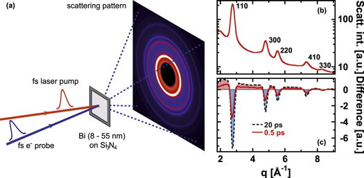
Figure 1. (a) Schematic of the experimental geometry. Thin Bi films deposited on free-standing Si3N4 membranes are irradiated with 60 fs, 800 nm laser pulses (near normal incidence). Their structural response is probed by diffraction of 300 fs, 4.2 MeV electron pulses in normal incidence transmission geometry. (b) Scattering intensity I(q) as a function of momentum transfer q of a 15 nm Bi film. (c) Difference scattering pattern  (
( unpumped) for delay times
  = 0.5 ps (red) and
  = 20 ps (black).
Download figure:
Standard image High-resolution imageSamples comprised polycrystalline, (003)-textured (heaxagonal notation) thin films of Bi with 8 nm, 15 nm, 25 nm and 55 nm thickness, respectively, grown on free standing amorphous Si3N4 membranes supported by a Si wafer frame using a home-built high-vacuum MBE system operated at a base pressure below 10−8 mbar. Before deposition the substrates were degassed at 265o C for several hours. Bi (99.999% purity) was deposited from an e-beam heated crucible while the sample was kept at room temperature. The film thickness was measured during deposition with a quartz crystal monitor placed next to the sample, which was calibrated separately with ex situ AFM. While this ensures a high accuracy of the relative film thicknesses as well as very good reproducibility from deposition to deposition, the absolute coverage is accurate only to approximately 10%. To compensate for slight surface oxide formation during the subsequent transport through air [33] each film was grown 3 nm thicker as the quoted thickness.
3. Results and discussion
Figure 1(b) depicts as an example the diffracted signal I(q) of a non-excited 15 nm Bi film as a function of momentum transfer  (
( de Broglie wavelength, θ: scattering angle) obtained by azimuthal integration (along lines of constant q) of the recorded scattering image. Due to the (003)-texture of the film and the very short de-Broglie wavelength (i.e. extremely flat Ewald-sphere) only five Bragg-reflections (hkl) with l = 0 of more than 90 allowed reflections are visible over the detected q-range. While this clears up the otherwise very dense diffraction pattern of Bi and enables to separate the individual Bragg-peaks, our experiment (similar to other UED-experiments on Bi [14, 17, 28]) is only sensitive to atomic motion perpendicular to the Bi c-axis/surface normal and thus neither directly affected by the coherently excited
  optical phonon [23–25], nor the excitation of longitudinal acoustic wave packets (e.g. [34]). This also allows to analyze the diffuse background between the Bragg-peaks which is caused by the thermal diffuse scattering of the Bi film (as well as by scattering of the amorphous Si3N4-substrate).
Figure 1(c) shows transient difference scattering pattern pumped–unpumped for two different pump–probe time delays  for the same film after excitation at a fluence of3
F = 0.69 mJ cm−2. An order-dependent decrease of the Bragg-peak intensities as well as an increase of the diffuse background is clearly visible. As will be discussed in detail below, both features can be attributed to the Debye–Waller effect and thus to an increase of the r.m.s. atomic displacement in the Bi film after sample excitation.
for the same film after excitation at a fluence of3
F = 0.69 mJ cm−2. An order-dependent decrease of the Bragg-peak intensities as well as an increase of the diffuse background is clearly visible. As will be discussed in detail below, both features can be attributed to the Debye–Waller effect and thus to an increase of the r.m.s. atomic displacement in the Bi film after sample excitation.
3.1. Transient Debye–Waller effect
For a quantitative analysis the integrated signal of the Bragg-peaks has been determined as a function of pump–probe time delay Δt by fitting each peak separately with a Gaussian function superimposed on a (linear) background. Figure 2(a) shows as an example the result of such an analysis for the same 15 nm Bi film and the same pump fluence of F = 0.69 mJ cm−2 as in figure 1(c); the integrated diffraction signal has been normalized to the value measured at negative delay times, i.e. before sample excitation. Figure 2(a) also contains (as violet data points) the time dependence of the diffuse scattering signal measured over an intervall  =
=  Å−1.
Å−1.

Figure 2. Transient diffraction data for a 15 nm Bi film. (a) Normalized integrated diffraction efficiency of various Bragg-peaks (hk0) as a function of pump–probe time delay for an excitation fluence F = 0.69 mJ cm−2; the violet data points show the time dependence of the diffuse scattering signal measured at  Å
Å (b) Asymptotic logarithmic intensity change (signal averaged over the delay range 12 ps
 15 ps) as a function of the squared momentum transfer
  (compare (1b)) for various excitation fluences (color-coded as labelled in figure 2(c)), the open red symbols correspond to the data shown in (a)). Inset: asymptotic r.m.s. atomic displacement change
  perpendicular to the Bi c-axis as a function of pump fluence as obtained from the slope of the linear fits to the data in (b); the temperature scale refers to the temperature dependence of the r.m.s. displacement reported by Arnaud et al [35]. (c)
  as a function of pump–probe time delay for various excitation fluences.
Download figure:
Standard image High-resolution imageAs already mentioned above, the integrated diffraction signal of the Bragg-peaks exhibits an order-dependent decrease within a few ps, while the diffuse scattering increases on a similar time-scale. Within the Debye–Waller model the intensity decrease of l = 0 Bragg-peaks  is caused by the increase of the r.m.s. atomic displacement perpendicular to the c-axis4
 and can be expressed as:


Herein  denotes the scattering signal of the unpumped sample (measured at negative time delays) and Ghk0 the length of the reciprocal lattice vector corresponding to reflection (hk0). Equation (1b) is particularly useful to verify whether the experimental data can be described within the Debye–Waller model: plotting the negative logarithm of the normalized intensity as a function of
  should result in a linear dependence with a slope determined by the increased r.m.s. displacement
Figure 2(b) shows this dependence for the the asymptotic intensity  (signal averaged over the delay range 12 ps
 15 ps) as a function of
  for different fluences (color-coded as labelled in figure 2(c)). The measured data follow indeed the linear behavior expected from the DW-model indicating that the lattice excitation perpendicular to the c-axis is dominated by incoherent, statistical atomic motion. From the slope of linear fitting curves (solid/dashed curves) the corresponding asymptotic r.m.s. displacement
  has been determined, which is shown in the inset of figure 2(b) as a function of pump fluence. The dashed curve represents a quadratic fit to the data indicating a slight non-linearity in the degree of lattice excitation with fluence.
It should be emphasized that the linear functions used to fit the measured data intersect the origin, a direct consequence that diffraction of MeV electrons can be described in the kinematic limit for these sample thicknesses. At non-relativistic energies experiments have frequently shown a finite intercept with the ordinate in dependencies similar to figure 2(b) [40, 41] and/or exhibit direct beam (zero order) attenuation [41, 42].
We verified that the DW-model does not only describe the asymptotic late time behavior but the experimental data for all delay times, giving evidence that coherent contributions to the atomic motion (perpendicular to the c-axis) are negligible even directly after excitation. Such coherent contributions, i.e. an excitation of the  optical phonon mode, can in principle occur by stimulated Raman-scattering [43] and, for stronger excitation, via anharmonic coupling to the displacively excited
  mode (motion along the c-axis) [44]. Time-resolved x-ray diffraction measurements [45] have however shown, that the coherent excitation of the
  -mode is weak and strongly damped, which has been explained by the very short lifetime of the electronic states driving the mode [46, 47]. Therefore, the diffraction data can be used to determine
  as a function of delay time. As an example figure 2(c) shows
  measured on the same 15 nm Bi film as before for different fluences.
Frequently r.m.s. displacements measured in time-resolved diffraction experiments are used to derive an induced lattice temperature rise  [14, 40, 41, 48] implying thermal occupation of the phonon modes of the system. For Bi this is a reasonable assumption only for long time delays after full electron-lattice equilibration (see below [27, 35]). Therefore, we only converted
  into a temperature (see left ordinate in the inset of figure 2(b)). This requires knowledge of the temperature dependence of the Debye–Waller-factor at high temperatures. With the Debye–Waller factors reported by Fischer et al [38] for temperatures of 294 K and 516 K, respectively, and assuming a Debye-like linear increase with temperature our measured
  yield unrealistically high temperatures (e.g.
  = 400 K at F = 1.1
  well above the melting point). Alternatively, using a Debye temperature of
  K, as derived from x-ray diffraction measurements at room temperature [39] (equivalent to the parametrized temperature dependent Debye–Waller factor reported by Gao et al [49]), more realistic, lower
  are obtained, but still the final temperature is in excess of the melting temperature at the highest fluences. In contrast, using transmission electron diffraction a much lower Debye-temperature of
  K has been found for Bi nanoparticles by analyzing the temperature dependent decrease of the (110) Bragg-peak intensity [50]. Applied to our data this would result in a correspondingly smaller laser-induced temperature increase (e.g.
  = 180 K at F = 1.1 mJ cm−2). The temperature estimates shown in figure 2 are based on the results of first principle calculations by Arnaud and Giret [35] (compare their figure 2(b)) yielding a maximum temperature close to the melting point at F = 1.1 mJ cm−2, the highest fluence we were able to perform measurements. When the fluence was increased above 1.1 mJ cm−2 accumulative sample damage was observed as evidenced by a progressive permanent reduction of the Bragg-peak intensities.
3.2. Phonon softening and squeezing
Electronic excitation of Bi leads to rather strong changes of the interatomic forces and thus to phonon softening, as has been first observed for the  optical mode through time-resolved reflectivity measurements [51, 52]. DFT calculations have shown that phonon softening extends over large parts of the Brillouin zone [22]. Using sub 100 fs laser pulses for excitation it occurs on a time-scale short compared to even the highest frequency modes and induces a squeezed phonon state [27] where the initial room temperature r.m.s. displacement is too small in relation to the weakened interatomic forces. The system relaxes by a rapid increase of the r.m.s. displacement within a few hundred fs [27, 35], as demonstrated by the data depicted in figure 3 showing
  measured with finer delay stepping on a 15 nm Bi film for an excitation fluence of 1 mJ cm−2.
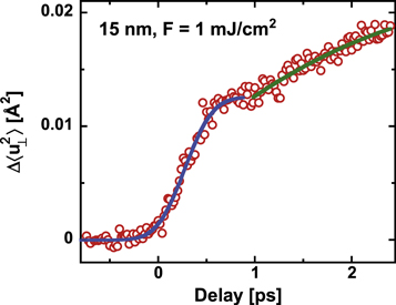
Figure 3.
 as a function of pump–probe time delay measured with finer delay stepping on a 15 nm Bi film for an excitation fluence F = 1 mJ cm−2. The blue and green curves (guide to the eye) represent the response due to the initial relaxation of the squeezed phonon state and ordinary electron–phonon coupling, respectively.
Download figure:
Standard image High-resolution imageThese data very clearly evidence a two-step evolution in the lattice response with a very fast sub-ps component (blue curve; guide to the eye) subsequently followed by the relaxation towards the final equilibrated state (green curve) which is reached on a few-ps time-scale (see figure 2). Following the interpretation of Johnson et al [27] we associate the initial component with the dynamics of the squeezed phonon state while the slower response is due to ordinary electron–phonon coupling and the transfer of electronic excess energy to the lattice.
We would like to note that the generation of squeezed phonon states as a result of electronically induced changes of the interatomic forces [53] is a more general phenomenon and has been used to map phonon dispersion relations [54] and identified as a precursor of non-thermal melting in covalent semiconductors [55]. Bi with its Peierls-distorted equilibrium structure exhibits a pronounced sensitivity to electronic excitation. Therefore, lattice softening and squeezing effects are particularly strong: the initial increase of the r.m.s. displacement amounts to approximately 40% of the total  . Moreover, even after relaxation of the squeezed state
  cannot be directly converted into changes of the lattice temperature
  since both, the amount of energy that is transferred from the excited electronic system to the lattice and the inter-atomic forces change with time during electron-lattice equilibration. Within a simple Debye-picture where
  (
( ) the Debye-temperature
  is not a constant but depends on the degree of electronic excitation (e.g. electronic temperature [35]) and is, therefore, a time-dependent quantity.
3.3. Thickness dependent relaxation
Qualitatively similar results as discussed so far for 15 nm films have been obtained also for Bi films with 8 nm, 25 nm and 55 nm thickness. All samples exhibit a two-step temporal evolution of the r.m.s. displacement with a 'fast' (softening/squeezing) and 'slow' (electron-lattice energy exchange) component. While the speed of the initial 'fast' increase is limited by the temporal resolution of the experiment, the "slow" response caused by electron-lattice relaxation exhibits a pronounced thickness dependence. This is demonstrated by the data shown in figure 4.
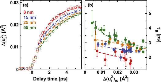
Figure 4. (a)  as a function of pump–probe time delay for Bi films of different thickness (red: 8 nm; blue: 15 nm; orange: 25 nm; green: 55 nm). In all cases the same asymptotic r.m.s. displacement
  Å2 is reached at long delay times. The dashed curves represent exponential fits to the data for
  0.8 ps. (b) Equilibration time
  for Bi films of different thickness as a function of the asymptotic r.m.s. displacement
Download figure:
Standard image High-resolution imageFigure 4(a) compares time-dependencies of  which lead to the same (within the experimental error) asymptotic r.m.s. displacement
  Å2, for the four different film thicknesses. To quantify the speed of electron-lattice equilibration by an energy relaxation time
 these time dependencies have been fitted by an exponential increase (dashed curves). Only data measured at delay times
  0.8 ps have been taken into account in order to clearly separate energy relaxation from the initial squeezed state dynamics. For the examples shown in figure 4(a)
  decreases from 3 ps for the 55 nm thick film to 1.8 ps at 8 nm thickness. While these values are in principal agreement with previously reported results [14, 15, 17] our data give clear indication for an increased electron–lattice coupling with decreasing sample thickness. This conclusion is confirmed by figure 4(b) which shows
  as determined from a large number of measured
  (more than 90 delay scans) for the different sample thicknesses as a function of
  . Despite fluctuations in the data it is evident that electron-lattice equilibration becomes faster at stronger excitation and, in particular, with decreasing film thickness.
Let us first comment on the observed decrease of  with increasing excitation strength. Indications for a fluence dependent energy relaxation in Bi have been reported before [14, 15], but only over a very limited range of fluences. Such behavior can be attributed to electronic density of state effects [56, 57], which are expected to be particularly strong in Bi [35] since the electronic density of states is low at the Fermi-level but increases significantly at higher energies—states that are occupied for the high excitation levels used in the experiments here.
With respect to the observed thickness dependence it has to be stressed that time-resolved x-ray diffraction experiments [25] have revealed an effective energy deposition depth of approximately 26 nm at similar excitation fluences, which is larger than the optical absorption depth of Bi ( at λ = 800 nm [58]). Furthermore, ambipolar electron-hole-diffusion leads to a distribution of the deposited energy deeper into the sample. Using a diffusivity D = 2.3 cm2 s−1[25], we estimate a diffusion length of about 15 nm during the first ps after excitation. Therefore, a homogeneous excitation profile prior to electron-lattice equilibration can be assumed for film thicknesses up to at least 25 nm and, therefore, the thickness dependent energy relaxation can not be attributed to transport effects within the film (which might play a role for the 55 nm film).
To explain the thickness dependence we refer to work on the thermal boundary conductance (Kapitza conductance) of metal–insulator interfaces. For these systems it has been proposed that direct coupling of metal electrons to phonons of the insulating substrate provide an additional channel for energy transport across the interface [59, 60]. Experiments on thin Au-films have provided evidence that this effect might be particularly effective as long as electrons and lattice are not in equilibrium [61, 62]. It will lead to a faster cooling of the hot electrons in the film and thus also to faster equilibration with the lattice. Since it is an interface effect its absolute magnitude does not depend on film thickness, but its relative weight will increase with decreasing thickness which accelerates the equilibration in thinner films, as observed in our experiments.
In a simplified picture we may decompose the total equilibration rate  into a bulk contribution due to the direct electron–phonon coupling
  in the Bi film and a contribution
  from the coupling across the interface to substrate phonons, as schematically shown in figure 5(a). While for given excitation conditions
  is independent of the film thickness d, the interface contribution is thickness dependent as
  [63], which leads to:


Figure 5. (a) Decomposition of the total equilibration rate  into a bulk contribution due to the direct electron–phonon coupling
  in the Bi film and a contribution
  from the coupling across the interface to substrate phonons. (b) Total equilibration rate
  as obtained from the time constants
  of the exponential fits to the data presented in figure 4(a) (same color coding of film thickness as in figure 4); the gray dashed line represents a linear fit according to (2).
Download figure:
Standard image High-resolution imageFigure 5(b) shows the total equilibration rate  —obtained from exponential fits to the time dependencies of
  depicted in figure 4(a)—as a function of the inverse film thickness. The measured data exhibit indeed a linear dependence as predicted by (2). This supports the interpretation of an interface-mediated contribution to the relaxation dynamics in thin films and allows to separate both parts. From the parameters of a linear fit (gray dashed curve) the bulk equilibration time can be determined as
  For the given case the interface contribution
  exceeds
  at film thicknesses below 10 nm highlighting the importance of this relaxation channel at nanoscale system dimensions.
4. Summary
In summary, ultrafast time-resolved transmission electron diffraction with short MeV electron pulses has been used to study electron-lattice equilibration in thin Bi films after fs optical excitation. Detailed and precise measurements of the transient Debye–Waller effect over an extended range of excitation fluences and for various film thicknesses allowed us to separate different contributions to the incoherent response of the lattice and to address explicitly the question whether the film thickness influences the relaxation dynamics.
Our data provide clear evidence for an accelerated electron-lattice equilibration with decreasing film thickness. The observed behavior can be explained by cross-interfacial coupling of hot electrons in the Bi film to phonons in the substrate. Our work demonstrates that ultrafast diffraction with such bright, ultrashort electron beams provides new opportunities to study structural dynamics in nanoscale materials. Future improvements of the source towards shorter pulses and increased brightness [32] will extend these exciting possibilities further.
Acknowledgments
This work was supported in part by the US Department of Energy Contract No DE-AC02-76SF00515, DOE Office of Basic Energy Sciences Scientific User Facilities Division, the Materials Sciences and Engineering Division, and the SLAC UED/UEM Program Development Fund.
: Author Contributions
KST, XW, and HAD initiated the project and conceived the experiment. DJ, CW, FMzH, and MHvH were responsible for sample preparation and pre-characterization. KST, RL, SPW, AHR, TC, and XW carried out the experiments. KST, FQ and ML analyzed the data. KST wrote the manuscript with specific contributions from ML, FMzH and XW, and comments from all other authors.
Footnotes
- 3
Incident fluences are quoted.
- 4
Due its crystal structure Bi exhibits directional anisotropy (with respect to the c-axis) in many of its properties (e.g. sound velocity [36]). However, room temperature diffraction studies indicate that the anisotropy of the r.m.s. displacement is negligible [37–39]. In contrast, studies at higher temperature give conflicting results. Fischer et al [38] report considerable anisotropy at 517 K, but with larger r.m.s. displacement perpendicular to the c-axis than parallel to it. This contradicts more recent results on Bi nanoparticles [15] as well as expectations based on the reported anisotropy of the sound velocity [36] with the c-axis being the 'softer' direction. To avoid any ambiguitiy, we restrict the discussion to the observable of our experiment, namely the r.m.s. displacement
 in the basal plane perpendicular to the c-axis. If one assumes isotropy the total .

