


Abstract
The possibility of investigating macroscopic coherent quantum states in polariton condensates and of engineering polariton landscapes in semiconductors has triggered interest in using polaritonic systems to simulate complex many-body phenomena. However, advanced experiments require superior trapping techniques that allow for the engineering of periodic and arbitrary potentials with strong on-site localization, clean condensate formation, and nearest-neighbor coupling. Here we establish a technology that meets these demands and enables strong, potentially tunable trapping without affecting the favorable polariton characteristics. The traps are based on a locally elongated microcavity which can be formed by standard lithography. We observe polariton condensation with non-resonant pumping in single traps and photonic crystal square lattice arrays. In the latter structures, we observe pronounced energy bands, complete band gaps, and spontaneous condensation at the M-point of the Brillouin zone.
Export citation and abstract BibTeX RIS

Content from this work may be used under the terms of the Creative Commons Attribution 3.0 licence. Any further distribution of this work must maintain attribution to the author(s) and the title of the work, journal citation and DOI.
Exciton polaritons are an ideal system for studying the collective behavior of macroscopic coherent quantum states in a solid-state environment [1]. The possibility of engineering polariton trapping potentials [2] has triggered interest in using polaritonic systems to simulate complex many-body phenomena, such as the physics of high-temperature superconductors, graphene, and frustrated spin lattices [3–5]. Quantum simulators are envisaged as a highly desirable tool for understanding complex many-body properties of novel solid-state, chemical, and biological systems, which are otherwise difficult to access. Quantum simulations rely on the emulation of Hamiltonians via potential landscape engineering in a highly controllable quantum system [6]. Ultracold atoms are superb candidates for quantum simulation schemes [7] since modern techniques allow for arranging them in optical lattices with high precision, leading to spectacular observations such as simulating the physics of a quantum phase transition in a Bose-Hubbard system [8]. However, a system based on cold atoms needs to operate at very low temperatures in the nK-μK range, it can hardly ever be fully scalable, and its integration is difficult due to the requirement of careful isolation from the environment. Polariton gases in microcavities have been identified as promising candidates for solid-state quantum simulators, as they fulfill a range of important prerequisites. First of all, they can form bosonic condensates [9, 10], which implies a macroscopic occupation of a single energy state close to thermal equilibrium [9]. Furthermore, they can enter a superfluid phase [1, 11, 12], possess internal (pseudo-spin) degrees of freedom [13], can be localized by lithographic [2] or optical techniques [14] possibly down to the single-polariton level [15], and their interaction constants are tunable [13]. An ideal trapping technique for the implementation of polariton quantum emulation should combine the following features: (i) the confinement depth should be tunable in a wide range; (ii) inter-site coupling should be readily controllable; (iii) surface recombination effects from etching the active medium should be avoided completely. None of the previously implemented approaches to observing polariton condensation phenomena in lattice structures have fulfilled all these important conditions: the shallow potentials provided by metal structures on planar microcavities typically are insufficiently strong to open complete band gaps in 2D configurations [2], and can hardly ever provide single on-site polariton localization. The confinement provided by etched pillars [4] resembles an infinitely high hard-wall box due to the etched sidewall, which makes the inter-site coupling strength rather difficult to engineer and control. Furthermore, due to the deep etching through the quantum wells, a strong background signal from uncoupled excitons, which are strongly broadened by surface and strain relaxation effects, is commonly observed, which can degrade the polariton emission signals, in particular for small sizes and at moderate exciton-photon detunings. Acoustic lattices [16] can provide deep and tunable potentials, but they are of a dynamic nature and cannot be implemented in arbitrary geometries.
Here we employ a technology that enables deep (several meV) potentially tunable trapping in any 2D geometry without affecting the favorable polariton characteristics. The traps are based on a locally elongated microcavity which can be formed by standard lithography. We observe polariton condensation under non-resonant pumping in single traps and photonic crystal square lattice arrays. In the latter structures, we observe pronounced energy bands, complete band gaps, and spontaneous condensation at the M-point of the Brillouin zone.
The concept of confining polaritons in locally elongated cavity regions (we will call them polariton mesa traps in the following) has been introduced by El Daif et al [17] and theoretically analyzed [18]. To generate a condensate of polaritons in such structures, however, we have had to significantly modify the sample scheme, as we describe in the following.
The epitaxial layer structure of our sample is shown in figure 1(a). It consists of an AlAs/AlGaAs microcavity with eight quantum wells, which are distributed over two stacks. One stack is integrated into the optical antinode of a  thick AlAs cavity layer; the second stack is located at the first AlAs/AlGaAs interface in the bottom distributed Bragg reflector (DBR). After the growth of the bottom DBR and the AlAs cavity, a 10 nm thick GaAs layer caps the cavity structure to protect it from fast oxidation of the aluminum containing layers. The vertical position of this spacer is chosen to coincide with an optical node in the complete structure. Following the growth of the bottom part of the sample, the wafer is removed from the molecular beam epitaxy system, and small mesa structures with heights of 5 nm to 30 nm are patterned into the cavity layer via electron beam lithography and wet chemical etching. Afterwards, the sample is reinstalled in the molecular beam epitaxy reactor and, after a cleaning procedure with activated hydrogen, the top DBR is grown. The buried mesas, which are schematically shown in figure 1(b), provide optical confinement which is sufficiently strong to localize the exciton-polaritons. This is directly manifested in the photoluminescence images in figures 1(c) and (d), obtained by pumping the microcavity with a laser frequency far above the exciton resonance.
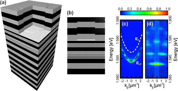
Figure 1. QW-microcavity polariton trap sample. (a) Schematic drawing of the mesa trap structure for providing lateral confinement for polariton condensates. (b) Drawing focused on the active region showing an overgrown trap. (c) and (d) Energy-momentum dispersion of a trap with a diameter of 30 μm and 4 μm respectively. In (c) a fit to the lower polariton dispersion (dashed black line) and the corresponding bare photonic dispersion (dashed white line) is shown.
Download figure:
Standard image High-resolution imageAt the quasi-planar regions of the wafer (figure 1(c)), the energy-momentum dispersion is characterized by a smooth parabola. The shape of the parabola can be reproduced by the planar dispersion of a lower polariton (LP) with a Rabi splitting of ERS = 11.5 meV and a cavity-exciton detuning of Δ = EC(k|| = 0) − EX(k|| = 0) = −12.3 meV. For mesa sizes <20 μm we systematically observe quantized modes as a result of the finite size of the structure (see the supplementary material for a detailed analysis), as depicted in figure 1(d) for a mesa with a diameter of 4 μm. The depth of this confinement is estimated at ∼55 meV for an etchdepth of 30 nm.
We first assess the possibility of generating a polariton condensate in very large mesas with a diameter of 50 μm, i.e., much larger than our pump spot. The corresponding dispersion images are shown in figures 2(a)–(c) for low to high excitation conditions, respectively. The cavity–exciton detuning of this device was extracted to be Δ = −11.6 meV, i.e., on the order of the Rabi splitting, which corresponds to an excitonic fraction of 14% and leads to a modest line broadening as compared with the pure photonic case (see the supplementary material). By increasing the excitation power, we observe a strong modification of the dispersion and a pronounced emission from the energy ground state. This transition is accompanied by a clear threshold in the input-output characteristics (figure 2(d)), a persisting continuous blueshift of the energy ground state (figure 2(e)), and a drop in the emission linewidth followed by some broadening as a result of polariton decoherence via self-interactions for higher densities (figure 2(f)). These features are commonly attributed to the formation of a polariton condensate [9, 19].

Figure 2. Polariton condensate formation in large traps. (a)–(c) Energy–momentum dispersions with false-color intensity profiles corresponding to excitation powers of 0.2, 1.0, and 1.3 times power at the condensation threshold Pth = 3.0 mW. Below threshold (a), the polaritonic system is characterized by a thermal distribution of particles. High ground-state population is observed above the polaritonic condensation threshold (c). (d) Input–output characteristics of the emission from the microcavity. (e) Ground-state energy and linewidth (f) as a function of the excitation power. The persisting blueshift across the threshold is a clear indication of polariton condensation formation. The linewidth decreases sharply when the threshold power is reached, a signature of temporal coherence.
Download figure:
Standard image High-resolution imageNext we carry out an in-depth study of a polariton trap with a diameter of 6 μm and a detuning of 3.9 meV. As a result of the deep confinement provided by the ∼30 nm high mesa, the energy states split into discrete levels which are strongly broadened in k-space (see the supplementary material for details of the energy structure), as can be seen in figure 3(a)–(c). Due to the deep confinement, the planar polariton dispersion is significantly detuned to a spectral range outside the detection window. In a manner similar to the previously discussed planar section of the microcavity, a strong occupation of the lowest energy state is observed for high pump power (figure 3(d) and 3(g)) along with a characteristic condensation threshold in the input–output characteristics, accompanied by a persisting blueshift of the energy ground state above threshold (figure 3(e)) and a sharp decrease in the emission linewidth at threshold (figure 3(f)). All these features, in particular the energy shift, which is linear below and logarithmic above the threshold, are in excellent agreement with previous reports on planar [20] and etched pillar polariton lasers [21]. We plot the normalized occupancy of the polariton states as a function of the energy in figure 3(g) on a semi-logarithmic scale. Due to the photonic confinement, the spectra feature pronounced photonic resonances. At threshold, we can reproduce the decay of the occupancy of the polaritonic resonances by a Maxwell-Boltzmann fit and extract a sample temperature of 38 K. Above the threshold power Pth a macroscopic ground state occupation builds up.

Figure 3. Polariton condensate formation in a zero-dimensional trap. (a)–(c) Energy–momentum dispersions with false-color intensity profiles corresponding to excitation powers of 0.3, 1.1, and 8.1 times power at the condensation threshold Pth = 2.5 mW for a mesa with a diameter of 6 μm. Below threshold (a), the polaritonic system is characterized by a thermal distribution of particles; in particular the first excited polariton state is clearly pronounced. High ground-state population is observed above the polaritonic condensation threshold. (b)–(d) Input–output characteristics of the emission from the microcavity. (e) Ground-state energy and linewidth (f) as a function of the excitation power. (g) Occupancy of the polariton traps as a function of the energy (normalized), indicating the formation of a condensate above the threshold.
Download figure:
Standard image High-resolution imageThe major advantage of our technique, as compared with optical trapping techniques, metal mask deposition, and etched pillars, is the possibility of creating polariton lattices based on deep potential traps with widely tunable coupling strength without etching the active medium. The band structure in a lattice configuration is determined by the overlap of the polariton wavefunctions between the neighboring sites. We demonstrate successful formation of polaritonic bands separated by well-defined gaps in a lattice composed of polariton traps with a diameter of 2 μm and a height of 5 nm arranged in a square lattice configuration. The arrangement is depicted in figure 4(a): the photonic confinement potential for this trap height amounts to ∼5 meV, and the fundamental mode is deeply confined (∼2.6 meV) below the continuum in the barrier (see the supplementary material). The polariton wavefunctions can penetrate into the barrier, leading to evanescent photonic coupling between neighboring sites, which is accompanied by the formation of a band structure. Using the linear exciton-photon coupling Hamiltonian [19], it can be shown that the structure of the energy bands imposed on the cavity photon mode by the periodic potential translates into the band structure of the polariton spectrum [18] (see the supplementary material). The band structure of the polariton energy can be derived from the single–particle states  in a periodic potential
  where a is the lattice period,
  is the Bloch function, and
  is contained within the first Brillouin zone (BZ). The energy eigenstates are found by solving the time-independent Schrödinger equation for

where n is the band index, and  the effective polariton mass, and the effective periodic potential for polaritons can be approximated by
 ![$V\left( {\bf r} \right)={{V}_{L}}[{{{\rm cos} }^{{}}}\left( {{k}_{L}}x \right)+{{{\rm cos} }^{{}}}({{k}_{L}}y)]$](https://content.cld.iop.org/journals/1367-2630/17/2/023001/revision1/njp507536ieqn8.gif) with kL = π/a. A typical structure of energy bands is plotted in figure 4(b) (assuming an effective polariton mass
with kL = π/a. A typical structure of energy bands is plotted in figure 4(b) (assuming an effective polariton mass  and a potential depth of 5.5 meV) along the main symmetry directions of the first irreducible BZ (see inset). The LP spectrum in the photonic crystal landscape acquires energy bands separated by gaps, and a complete gap opens between the M-point of the s-band (n = 1) and the X-point of the p-band (n = 2) for sufficiently deep lattice potentials. A comparison between experiment and theory is shown in figure 4(c), recorded for a lattice with a period of 3 μm below the condensation threshold from the
  to the X-point of the BZ. The wavefunction overlap is sufficient to form distinct bands for the three lowest energy levels, which can be perfectly reproduced by our model with realistic parameters:
  For larger lattice spacings (figures 4(d)–(f)), the coupling between the sites is successively reduced, leading to a strong increase in the effective mass of the polaritons in the lowest lying s-band and a pronounced tight-binding regime.
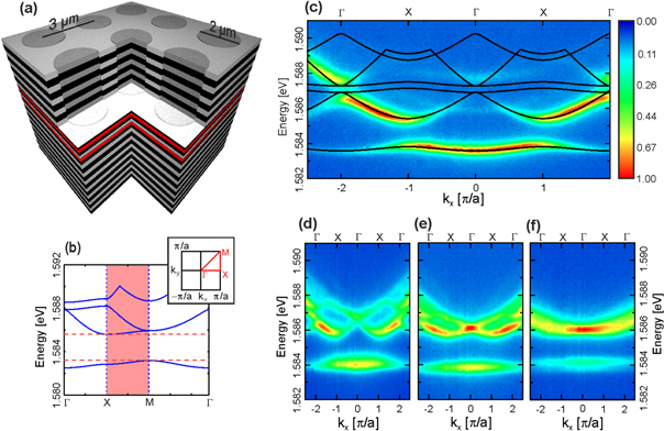
Figure 4. Polaritons in a square lattice. (a) Schematic drawing of the investigated square lattice structure consisting of buried polariton traps. (b) The first four energy bands for a square lattice array of polariton traps in the reduced BZ representation. The dashed lines indicate the position of the complete band gap. Inset: first irreducible BZ. (c) Photoluminescence spectra of a square lattice with a lattice constant (c) a = 3 μm, (d) 4 μm, (e) 5 μm, and (f) 7 μm recorded along the Γ–X symmetry direction. A reciprocal false-color scale is chosen (see (c)) for better visibility of the band structure. The axis shows the momentum in units of the BZ, whereas the upper axis marks the symmetry points. The band structure calculated theoretically is plotted in black lines in (c).
Download figure:
Standard image High-resolution imageTo assess the nonlinear characteristics of our polariton lattice structure, we perform a power dependent investigation of the square lattice structure shown in figure 4(c) at a slightly different detuning of −7.8 meV. We provide a close-up image of the gap between the s and p-bands in our system, taken along the X–M symmetry direction below (figure 5(a), P ∼ 0.2 Pth) and above (figure 5(b), P ∼ 1.3 Pth) the condensation threshold. Again, perfect agreement between experiment and theory is achieved for the same realistic parameters (adjusted for the difference in detuning). For a higher pump power, e.g., P ∼ 1.3 Pth, the condensation occurs in the vicinity of M-points of the BZ and the condensate energy blueshifts into the full gap of the linear spectrum due to the nonlinearity (see figure 5(b)). A detailed discussion of the phenomenon can be found in the supplementary material). This behavior suggests the formation of a spatially localized two-dimensional gap soliton state [22] previously predicted in square lattice potentials [23] and observed in potentials induced by surface acoustic waves [16]. Although these gap states are analogous to their 1D counterparts as observed in modulated photonic wires [24], the essential requirement for their existence in 2D is the complete gap being available only at the M-point in a sufficiently deep lattice. The sufficient width of the gap in our lattice enables detailed investigation of the gap soliton formation in the incoherent, off-resonant excitation regime at different pump powers (see the supplementary material). To investigate the spatial coherence properties of this state, we superimposed the real space emission of a 3 × 3 lattice cell on its mirrored image in a Michelson interferometer [25]. The excitation conditions were chosen so that a high emission intensity was reached, whereas the far-field dispersion characteristics were still similar to figure 5(b) (P ∼ 2.7 Pth). The resulting image (figure 5(c)) shows a distinct interference pattern throughout the cell, with high fringe visibility in the centered column of traps which is proportional to the first order correlation function.

Figure 5. Condensation in a square lattice. (a) Zoom onto the band gap region of a square lattice with a lattice constant a = 3 μm recorded along the X–M symmetry direction, revealing a complete gap between the M and X symmetry points of the first BZ. (b) For large pump power (1.3 Pth, with a condensation threshold Pth = 5.7 mW), polariton condensation in the full gap near the M-point is observed. (c) Interference pattern of the square lattice real space emission created by superimposing the real space image on its mirrored reflected image in a Michelson interferometer [25]. The ∼15 μm-diameter excitation spot (p ∼ 2.7 times Pth) is focused on the center trap, and the mirror axis is chosen along the Y-direction at X = 0.
Download figure:
Standard image High-resolution image
In conclusion, we have observed evidence for the formation of a polariton condensate in a buried, deep microcavity trap, which is supported by a persisting blueshift above the condensation threshold and a strong line narrowing. The potential depth of the device can be lithographically tuned by varying the etch depth, and potentially via electro-optical methods. Such polariton traps can serve to generate polariton condensates which are spectrally and spatially decoupled from the reservoir (e.g., by pumping the barrier around the trap) to generate polariton condensates of unprecedented coherence. This technology platform can furthermore be exploited straightforwardly to fabricate 'guiding' channels, interferometers, logic and memory elements, and routers which serve as building blocks for polaritonic integrated circuits [26].
In our current work, we extended the study to traps which are arranged in a square lattice configuration and observed strongly pronounced features of site-to-site coupling for small lattice constants and localized polariton modes for lattice constants exceeding the evanescent nearest neighbor coupling. The remarkable feature of our deep lattice is a complete gap between the M-point of the s-band and the X-point of the p-band of the energy spectrum. A complete gap in a two-dimensional periodic potential opens only above a certain depth threshold. The possibility of reaching this regime with our devices opens the way to investigations of topologically nontrivial states in more sophisticated lattice geometries. Polariton condensation in these lattice structures is observed in the full band gap near the M-point of the s-band, indicating the presence of a spatially localized gap state. A combination of such a potential landscape with one induced by a structured optical pump [27, 28] may enable the engineering of tailored nontrivial potentials, such as bi-partite or deliberately non-Hermitian lattices, because the depth of potential wells produced by both techniques can be comparable. We believe that our work thus represents an important step toward the implementation of quantum emulators in polariton systems.
Experimental section
Sample design and fabrication
The two investigated samples were grown by molecular beam epitaxy in an etch-and-overgrowth technique. First the bottom 37 AlAs/Al0.2Ga0.8As DBR stacks and the  AlAs cavity layer were grown on (100)-oriented GaAs substrate with a 10 nm thick GaAs layer on top to prevent oxidation. In the center of the cavity and the interface of the first DBR mirror pair a stack of four 7 nm thick GaAs QWs separated by 4 nm AlAs barriers was embedded. The entire 3-in wafer was patterned with alignment marks and large mesa structures via optical lithography and deep wet etching. These alignment marks served as reference points for the subsequent electron beam lithography step, where various geometrical formations of circular traps with varying diameters were defined. The patterns were then transferred into the semiconductor by wet etching using an aluminum layer as the etch mask. By controlling the dilution of the etchant and the time of the etch process, the etch depth and therefore the height of the traps could be varied. Sample A was produced using the GaAs QW as an etch stop, resulting in a depth of ∼30 nm, whereas in sample B the depth of ∼5 nm was within the GaAs capping layer. Prior to the overgrowth of the samples with a 32-pair DBR mirror, the Al mask was removed and activated hydrogen cleaning of the surface was carried out in the load-lock chamber of the molecular beam epitaxy system to remove surface oxides and contaminations at moderate temperatures (400 °C).
Experimental setup
A compact low-temperature setup was constructed, in which both spatially (near-field) and momentum–space (far-field) resolved spectroscopy and imaging were accessible. Photoluminescence was collected through a 0.4 NA microscope objective lens (20× magnification) and directed into an imaging spectrometer with a grating of 1200 grooves/mm via a set of relay lenses, projecting the proper projection plane onto the monochromator's entrance slit. The system's momentum space resolution was ∼0.05 μm−1 (∼0.5°), and its spectral resolution was ∼0.050 meV, with a nitrogen-cooled Si charge-coupled device as the detector. All spectra were recorded at a sample temperature of ∼5 K. Non-resonant photoluminescence excitation was achieved with a continuous-wave laser tuned into a Bragg minimum at a wavelength around 724 nm.
Acknowledgments
This work has been supported by the State of Bavaria and the Australian Research Council (ARC). The authors thank M D Fraser, N Y Kim, Y Yamamoto, and V D Kulakovskii for fruitful discussions. This publication was funded by the German Research Foundation (DFG) and the University of Wuerzburg in the funding programme Open Access Publishing.