


Abstract
We propose to create an effective magnetic field for photons in a two-dimensional waveguide network with strong scattering at waveguide junctions. The effective magnetic field is realized by imposing a direction-dependent phase along each waveguide link. Such a direction-dependent phase can be produced by dynamic modulation or by the magneto-optical effect. Compared to previous proposals for creating an effective magnetic field for photons, this scheme is resonator-free, thus potentially reduces the experimental complexity. We also show that such a waveguide network can be used to explore photonic analogue of integer quantum Hall effect for massless particles.
Export citation and abstract BibTeX RIS
1. Introduction
The concepts of an effective gauge potential and effective magnetic field for photons has been extensively explored in the past few years [1–3]. Such concepts have strong connections to the emerging interests in topological photonics [4–8], and have led to the developments of new capabilities for manipulating light, such as on-chip optical isolators [9], topologically protected one-way edge states [10–16], as well as gauge-field induced negative refraction [17] and waveguiding [18].
In typical proposals for achieving effective magnetic field for photons [2, 3, 15, 16], one consider an array of resonators as described by a tight-binding Hamiltonian, with the coupling constants between the resonators exhibiting direction-dependent phases. In these proposals, the effective magnetic field in fact arises solely from the direction-dependent phases, and the resonators themselves play no essential role with respect to the effective magnetic field, other than perhaps simplifying theoretical treatments by allowing the use of a tight-binding model. On the other hand, in experimental systems, the use of resonator array places a very strong constraint on the practical implementation and applications. For example, the resonators themselves typically impose a stringent constraint on the operating bandwidth.
In this paper we propose a resonator-free scheme for generating an effective magnetic field for photons. We show that the waveguide network, as proposed in [19], can be used as a platform for implementing the mechanism for creating an effective gauge field. Using the transfer matrix formalism that describes the waveguide network system, we demonstrate robust one-way edge states and Hofstadter butterfly spectrum as evidence of an effective magnetic field for photons in these waveguide networks. This proposal eliminates the potential experimental complexity introduced by the resonators.
Furthermore, the network system provides additional flexibility in exploring new physics associated with photonic gauge field. For example, by designing the scattering matrix at the waveguide junction, the network may exhibit a Dirac-like dispersion in the absence of an effective magnetic field [19]. As a result, the behavior of the photonic states mimics the quantum Hall effect of a linear dispersion system (such as a single layer graphene), and differs from that of a quadratic dispersion system one usually get from a tight binding model on a square lattice.
This paper is organized as follows: section 2 describes the physical model of the waveguide network system, and possible implementations of the waveguide junction and the direction-dependent phase on waveguide links. Section 3 summarizes the band structure of a reciprocal waveguide network system. Section 4 introduces a uniform magnetic field into the waveguide network by adding direction-dependent phases on waveguide links. We present the dispersion and transport behavior of the resulting topologically protected edge states. Section 5 calculates the Hofstadter butterfly for the waveguide network system, and explores its connection to the Dirac-like underlying dispersion. We summarize in section 6.
2. Physical model for waveguide networks
Throughout this paper we will consider a class of waveguide network system as shown schematically in figure 1(a). The system consists of a square lattice of four-port waveguide junctions. These junctions are connected into a network via a set of waveguide links. Such a system has been analyzed previously by Feigenbaum and Atwater in [19], who envision a waveguide network system based on metal-insulator-metal waveguide structures (figure 1(b)) [20]. Similar waveguide networks can also be constructed for radio frequency (RF) photons using transmission lines or microstrip lines, or in the optical frequency range using dielectric waveguides [21]. Unlike Feigenbaum and Atwater, here we seek to create an effective magnetic field for photons, by introducing a non-reciprocal direction-dependent phase along each waveguide link.

Figure 1. (a) Conceptual drawing of the waveguide network. The pink dots represent waveguide junctions acting as four-port power splitters. The black lines represent waveguide links. The blue boxes represent components that generate a direction-dependent phase for photons propagating through the waveguide link. (b) A possible implementation of a waveguide network without the non-reciprocal phase using a plasmonic metal–insulator–metal wave network, based on the original proposal in [19]. The yellow regions represent metal. The white regions represent a dielectric such as air. (c) The waveguide junction and the labeling of various input and output wave amplitudes at the waveguide junction. (d) The labelling of input and output amplitudes at a waveguide link and the definition of the reciprocal ( ) and non-reciprocal (
 ) phase shift. (e) The dynamic modulation scheme for the generation of a direction dependent phase. Two mixers (circles with crosses) are driven by local oscillators with phases difference
  . The difference between the local oscillator phase defines the direction-dependent phase. (f) The magneto-optical scheme for the generation of direction-dependent phase. A magneto-optical material is incorporated into a normal waveguide and external magnetic field is applied to split the forward and backward propagating modes.
Download figure:
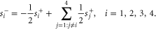
Standard image High-resolution imageIn this work, we consider a four-port junction described by the following scattering matrix S:


Here, (x,y) labels the position of the junction. The incoming and outgoing amplitudes along four waveguides connected to the junction at (x,y) are denoted as  ,
,  ,
,  ,
,  and
and  ,
,  ,
,  ,
,  , respectively, as shown in figure 1(c). The waveguide junction is described mathematically by a scattering matrix S in equation (2). Here
  is the reflection coefficient, and t is the transmission coefficient into a single outgoing waveguide. r and t are both assumed to be real. Here we assume a fully-symmetric S matrix. The form of the S-matrix is further constraint by energy conservation and time-reversal symmetry. Energy conservation requires that
  .
.
In the waveguide network considered here, when the power splitting into all four output ports are comparable in amplitude, any closed loop of connected waveguides demonstrate strong interference and resonance effect. The coupling of these non-local interferences and resonances enriches the network dynamics and tunability. Such power splitting behavior in the waveguide junction can be easily achieved when the cross section of the waveguide and the dimension of the junction is smaller than the wavelength, as in the cases of plasmonic metal–insulator–metal waveguides [19, 20], RF transmission lines and microstrip lines. In these systems the junction acts like a point-scatterer with equal scattering amplitude into all output ports. Furthermore, such a scattering matrix can be achieved with design of dielectric waveguide structures, for which both the waveguide and the junction are at the single wavelength scale [21].
Since most previous works on the effective gauge field for photons have utilized arrays of resonators [2, 3, 15], here we briefly comment on the connection between a waveguide network and a resonator array. The waveguide junction as shown in figure 1(a) can be realized with a resonator coupled equally to the four waveguide ports. In this case, the transmission and reflection can be calculated using coupled mode theory [22], which relates the incoming and outgoing wave amplitude  and
and  in the four ports to the amplitude of the resonant mode b

Here  is the resonance frequency.
  is the amplitude decay rate of the resonator to one of the waveguides. From equation (3) we can solve for
  in term of
  at a given frequency ω

and then obtain the scattering matrix of the junction. For the resonant case  , equation (4) simplifies to
The scattering matrix therefore has exactly the same form as in equation (2) with t = 0.5 and r = 0. Thus, the behavior of the waveguide network can be realized alternatively by considering a resonator array operating near resonance. In previous works on the effective gauge field for photons using a resonator array, the system is always operating close to resonance. However these resonators have very limited bandwidth. The waveguide junction studied here reproduces the behavior of a resonator operating on-resonance, but has a much larger bandwidth since the scattering matrix can be largely frequency-independent.
For the resonator case, at frequencies away from  , if we define
  and absorb the phase of the coefficient
  into the definition of
  , equation (4) becomes
This is equivalent to the scattering matrix in equation (2) once we define

Thus the waveguide junction with  represents a resonator operating off-resonance. The scattering matrix in equation (2) used to describe the waveguide junction can also map to resonator arrays operating on and off resonance.
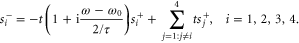
Next we look at the waveguide link. Here we assume that the waveguide link has no scattering between the two propagation directions, such that

where  is the reciprocal phase, as was also used in [19]. Here a is the length of each waveguide link. In this work, for simplicity we use a linear dispersion
  where v is the phase velocity in the waveguide. A more general dispersion relation will not change the essence of our result. Unlike [19], however, here we also include a non-reciprocal phase shift
  . The two directions of propagation have opposite non-reciprocal phases. The non-reciprocal phases are introduced to create an effective magnetic field for photons in the waveguide network.
Experimentally, the non-reciprocal phase can be introduced either with the use of dynamic modulation or with the use of magneto-optical effects. With the dynamic modulation scheme, one achieves a non-reciprocal phase by cascading two mixers. The difference in the phases of the local oscillators provides the non-reciprocal phase (figure 1(d)). This scheme was theoretically proposed in [23] and experimentally demonstrated in [9, 24, 25]. Alternatively, the non-reciprocal phase can be achieved using magneto-optical waveguides (figure 1(e)), as discussed theoretically in [26] in the context of photonic gauge field, and demonstrated experimentally in [27]. We refer the readers to the cited references for details on the experimental implementation. To conclude this section we note that the basic ingredients of our waveguide network, i.e. the junction and the waveguide link that provides a non-reciprocal phase, have all been implemented experimentally before. One may therefore anticipate the possibility of integrating these components together into a larger network.
3. Summary of waveguide network properties
In this section we provide a summary of the photonic band structure of the waveguide network shown in figure 1(a), in the absence of an effective magnetic field. In the rest of this paper we will refer to such a band structure as the underlying band structure. A detailed discussion of the properties of such a waveguide network can be found in [19]. Here we focus only on those aspects that we will need for subsequent discussions.
Figure 2 shows the photonic band structure of a square lattice of waveguide networks. We assume the waveguide links are reciprocal by setting  in equation (5). We consider two different cases corresponding to t = 0.5 and t = 0.4 in equation (2). In both cases, the network supports four photonic bands, since each unit cell has four degrees of freedom corresponding to
  ,
,  ,
,  and
and  in equation (2). Among the four bands, two of them are flat, which correspond to localized resonant states in the network [30]. In the following we will focus on the two non-flat bands, which we will refer to as the upper and lower bands, respectively.

Figure 2. Band structure of an infinite waveguide network in the absence of the direction-dependent phase, in the first Brillouin zone (left) and along the symmetry directions of a square lattice (right). (a) t = 0.5 and r = 0. Note the triply degenerate Dirac-like point at the Γ point [28, 29] consisting of two crossing linear bands and a flat band. (b) t = 0.4 and r = 0.6. Note the existence of gap at the Γ point.
Download figure:
Standard image High-resolution imageFor t = 0.5 (figure 2(a)), the upper and lower bands touch at the Γ point, and the whole band structure is gapless. Furthermore, the dispersion is linear near the Γ point. For  (figure 2(b)), the degeneracy at the Γ point between the lower and upper bands is lifted, and the spectral width of both the upper and lower bands is compressed as compared to the case where t = 0.5. The band structure is gapped, and the dispersion near the Γ point becomes quadratic. Tuning the scattering amplitude t of the waveguide junction thus allow one to explore systems with photons that are either massless or massive near the Γ point.
4. Effective magnetic field and edge state transport in waveguide networks
In this section, we calculate the band structure of an semi-infinite stripe of waveguide network with a uniform effective magnetic field. We further demonstrate the edge state transport in a finite structure. In this section, we assume t = 0.5 in equation (2).
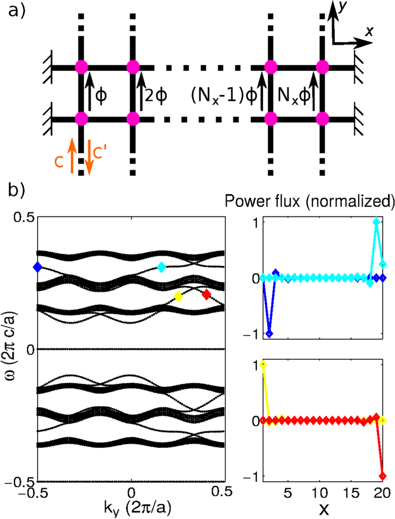
A uniform effective magnetic field for photons is introduced by imposing a specific arrangement of non-reciprocal propagation phases on waveguide links as shown in figure 3(a). Such an arrangement corresponds to the vector potential in the Landau gauge for a uniform magnetic field. All waveguide links along the x-direction do not have non-reciprocal phase, i.e.  . All waveguide links along the y-direction at the same x have the same non-reciprocal phase, and such a phase increases linearly as a function of x, i.e.
  . This produces an effective magnetic flux of ϕ per unit cell, and an effective magnetic field
  .
.

Figure 3. (a) A semi-infinite waveguide network with a uniform effective magnetic field. The phase on each vertical link denotes the non-reciprocal phase a photon accumulates as it propagates upward along the waveguide link. Downward propagation accumulates an opposite phase. The ends of the horizontal waveguides are truncated with a perfectly reflecting mirror. (b) Band structure and edge state power flux in the y-direction of a semi-infinite waveguide network with a width of  , and with magnetic flux
  per unit cell for t = 0.5. Using the labeling convention in figure 1(c), the power flux in the y-direction is
  .
.
Download figure:
Standard image High-resolution imageThe key effect of an effective magnetic field is the creation of topologically robust one-way edge states. Therefore, we consider the stripe geometry shown in figure 3(a). The stripe has a finite width in the x-direction, and is infinite in the y-direction. The waveguide links at the edges of the structure in the x-direction are truncated with a perfectly reflecting boundary condition. With our choice of spatial distribution of the non-reciprocal phases, the structure remains periodic in the y-direction. Therefore, its eigenstates can be characterized by a band diagram relating the frequencies ω to the wavevector ky along the y-direction. Such a band diagram is shown in figure 3(b), assuming that the stripe has a width of  , and
, and  , such that the magnetic flux through each unit cell is
  of the flux quanta
  . The flat bands from figure 2 remain unchanged, since they correspond to localized resonances in the waveguide network, and are unperturbed by the effective magnetic field. Since the magnetic flux through each unit cell is
  flux quanta, the corresponding infinite structure will have a periodicity of
  along the x-direction. As a result the lower and upper non-flat bands in figure 2 each splits into three groups of magnetic subbands. Band gaps occur between these magnetic subbands.
For each band gap between a pair of magnetic subbands, there are two one-way edge states whose dispersion span the entire gap as can be seen in figure 3(b). These two states have opposite group velocities. The spatial profile of these edge states can be visualized by calculating the distribution of power flux in the y-direction, which is  using the labeling convention in figure 1(b). This power flux distribution is plotted in figure 3(b). We see that the power flux is strongly localized on the edge, and that the two edge states in the same band gap are located on opposite edges of the stripe and propagate in opposite directions. These modes are the photonic analogue to the one-way edge states of electrons in the integer quantum Hall effect.
Having established the existence of the one-way edge states, we now consider their transport properties. For this purpose, we consider a finite waveguide network structure with a dimension of  by
by  , as shown in figure 4(a). The network structure is subject to a uniform effective magnetic field corresponding to
  . We terminate all waveguide ports at the edge of the structure with a perfectly reflecting boundary condition, except for the two ports at the upper-left and the lower-right corners, which act as the input/output ports. We inject the wave into the input port and extract the transmitted wave from the output port. For better visualization of the transport properties, we introduce a small loss at each waveguide link. The transmission per single pass through a link is assumed to be 99%, which corresponds to a single-pass loss of 0.087 dB per link. The transmission spectrum is plotted in figure 4(b). Transmission is significant at frequencies that lie within the band gaps spanned by edge states, and is suppressed at frequencies that lie either in the magnetic subbands or in the topologically trivial gaps.

Figure 4. Transport through a  by
by  block of waveguide network. (a) Illustration of the structure. All waveguide terminals are perfectly reflecting, except the input and output ports, as indicated by the green arrows. (b) Transmission as a function of frequency. The yellow regions indicate the frequency ranges of the magnetic subbands. The white regions correspond to the band gap regions. (c)–(f) Power flux distribution for forward (left) and backward (right) excitation, with input frequency marked by arrows in (b). Arrows in (c)–(f) indicate the input and output ports. Dash lines indicate waveguide links. Power flux is shown in red when going down or right, and blue when going up or left.
Download figure:
Standard image High-resolution imageFigures 4(c)–(f) shows the power flux distribution at four different frequencies. These frequencies are indicated by arrows in figure 4(b). The dashed lines indicate the waveguides, and the arrows indicate the input and output ports. The power flux along each waveguide link is represented by a color map superimposed on top of a schematic of the physical structure. Using the labeling convention in figure 1(c), the power flux in the horizontal waveguide links is defined as  , and the power flux in the vertical waveguide links is defined as
  . The power flux is represented in red when it goes down or right, and blue when it goes up or left.
When the excitation frequency lies within a gap spanned by edge states (figures 4(c) and (e)), the power flux is well-confined to the edge of the block and efficiently transmitted to the output port. In contrast, when the frequency lies within the magnetic subbands (figure 4(f)), the flux diffuses into the bulk of the block and is attenuated significantly. When the frequency lies within a trivial gap that does not have edge states (figure 4(d)), input flux barely penetrates into the bulk of the block and is mostly reflected.
In the left panel of figure 4(c), when light is injected from the top left corner and extracted from the bottom right corner, the power flux follows the left-bottom edge of the block, and it goes down and right. In the right panel of figure 4(c) where the input and output ports are switched from that of the left panel, the power flux follows the right-top edge of the stripe, and it goes up and left. This simulation result verifies that the two edge states lying within the same topologically non-trivial gap are located on opposite edges and travel in opposite directions, in consistency with the analysis of the semi-infinite stripe in figure 3.
Figure 4(c) is calculated for a frequency within the bandgap between the two lower subbands of the upper non-flat band of the underlying band structure. In contrast, figure 4(e) is calculated for a frequency within the bandgap between the two upper subbands of the lower non-flat band of the underlying band structure. The edge states in these two bandgaps have different chiralities. As a result the power flux flows anti-clockwise in figure 4(c) and clockwise in figure 4(e).
The presence of small amount of loss does not change the nature of the topological edge states. This is verified by the simulation shown in figure 4, in which a small loss on each waveguide link is included. In general, to demonstrate the effect predicted here, the propagation length needs to be on the order of a few structural periods. For plasmonic metal–insulator–metal waveguide, the propagation length of guided mode in near IR can be a few tens of microns [20]. Thus the periodicity needs to be on a single wavelength scale. Loss can be much lower in dielectric waveguide for optical frequencies or microstrip line for RF frequencies, which should allow structures with larger periodicities that might be easier to construct.
To summarize this section, by computing both the bandstructure and the transport properties we show that topologically protected edge states can be created using a waveguide network subject to a uniform effective mangetic field. The results show that non-trivial topology in photonic states can be achieved in a system without resonators.
5. Dirac-like dispersion
In section 3 we show that by tuning the scattering parameter t of the waveguide junction, the underlying bandstructure near the Γ point can be tuned from quadratic to linear and from gapped to gapless. The waveguide network can therefore be used to study the effect of a gauge field in both massive and massless systems. In this section, we contrast the behavior of the waveguide network under a uniform effective magnetic field between the massive and massless cases, by computing the Hofstadter butterfly pattern [31] in both cases.
In figure 5 we show the Hofstadter butterfly pattern for the waveguide network, under an uniform effective magnetic field. The horizontal axis is the magnetic flux Φ normalized to the flux quanta  . For each
  where
where  is a irreducible fraction, the system is periodic with a magnetic unit cell consisting of q unit cells of the waveguide network lattice in the absence of the effective magnetic field. Such a periodicity facilitates numerical calculations of the frequencies of the eigenstates. We plot the eigen frequencies in figure 5, with each black dot in figure 5 representing an eigen state of the waveguide network under a specific effective magnetic field. Clusters of black dots form magnetic subbands, separated by white patches representing bandgaps. In the lattice Hofstadter model, the lowest magnetic subband at small effective magnetic field (e.g. small
  ) should behave similarly to the lowest Landau level calculated from a continuous model. At small
  , the lowest magnetic subbands therefore should have near-zero bandwidth, as we indeed observe in figure 5.

Figure 5. Hofstadter butterfly for the infinite waveguide network (black) with a fitted curve to the lowest band (red). Only the upper half of the spectrum is shown for simplicity. (a) t = 0.5, and the red curve is a fit to  . (b) t = 0.4, and the red curve is a fit to a linear function
  , where
  is the lowest frequency of the band in the absence of the effective magnetic field.
Download figure:
Standard image High-resolution image
Figures 5(a) and (b) are calculated with different waveguide junction scattering amplitude t. Figure 5(a) corresponds to the case of t = 0.5, for which the underlying dispersion is Dirac-like (linear) at the Γ point as shown in figure 3(a). Consequently the frequency of the lowest magnetic subband at a small effective magnetic field is proportional to the square root of the effective magnetic field, e.g.  as shown with the red curve in figure 5(a), in consistency with [32–34] which explored integer quantum Hall effect in graphene. In contrast, figure 5(b) corresponds to the case of t = 0.4, of which the underlying dispersion is gapped and is quadratic near the Γ point as shown in figure 3(b). This system then behaves as a massive system, and the lowest magnetic subband has linear dependence on the effective magnetic field or
  , as shown by the red curve in figure 5(b). This behavior reproduces the standard behavior in integer quantum Hall effect for a free electron under magnetic field. The waveguide network system thus enables one to explore the effect of an effective magnetic field, for both massless and massive photons.
6. Summary
In summary, we propose a two-dimensional waveguide network with non-reciprocal phases as a resonator-free platform for realizing an effective magnetic field for photons, and demonstrate photonic analogue to the integer quantum Hall effect through band structure calculations and edge state transport simulations. In addition, we show that such a waveguide network can be used to study the effect of an effective magnetic field, on either massless or massive photons, by adjusting the power splitting ratio at the waveguide junction.
The waveguide network may prove to be a versatile platform for experimentally demonstrating the effective magnetic field for photons. It is free of some of the experimental constraints imposed by resonators, and it possesses rich tunability in its underlying dispersion.
This work is supported by an AFOSR MURI program, Grant No. FA9550-12-1-0488.