


Abstract
Cd3As2 is a new kind of three-dimensional (3D) Dirac semimetal with extraordinary carrier mobility, which can be viewed as '3D graphene'. Theory predicts that Cd3As2 can be driven into a quantum spin Hall insulator with a sizeable band gap by reducing dimensionality. In this letter, we report the systematic growth of undoped Cd3As2 thin films with the thickness of 50 ∼ 900 nm by molecular beam epitaxy. The magneto-transport study on these single-crystalline films shows a high mobility in the range of 3.8 ∼ 9.1 × 103 cm2 · V−1 · s−1 and a relative low electron concentration of 1 ∼ 8 × 1017 cm−3. Significantly, a thickness-induced semimetal-to-semiconductor transition was observed. In contrast with what is expected in the bulk counterpart, the 50 nm-thick Cd3As2 film exhibits semiconducting characteristics, witnessing an emerged bandgap opening when the dimensionality is reduced. Finally, the analyses on the temperature- and angular-dependence of magneto-resistance and Shubnikov-de Hass oscillations reveal a non-trivial to trivial Berry's phase transition that is in connection with the reduced dimensionality. Our results demonstrate that the Cd3As2 thin films with unique electronic structure and high mobility hold promise for Dirac semimetal device applications.
Export citation and abstract BibTeX RIS

Original content from this work may be used under the terms of the Creative Commons Attribution 3.0 licence. Any further distribution of this work must maintain attribution to the author(s) and the title of the work, journal citation and DOI.
Three-dimensional (3D) topological Dirac semimetals (TDSs), such as Na3Bi [1, 2] and Cd3As2 [3], have been theoretically predicted and experimentally realized in recent years. These TDSs have unique physical properties originating from 3D massless Dirac fermions. The Dirac nodes are developed due to the touching of valence and conduction bands at discrete points in the reciprocal space. Interestingly, for these 3D Dirac materials, they can be driven into various phases, such as Weyl semimetal [4] and topological insulator (TI) [5, 6] by breaking time reversal or inversion symmetry. Driven by these intriguing physical properties, extensive experiments on angle-resolved photoemission spectroscopy (ARPES) [7–10] and scanning tunneling microscopy (STM) [11] were carried out to identify the 3D Dirac fermions in these materials.
Cd3As2 is considered to be an excellent 3D TDS due to its chemical stability in air, and it also possesses novel transport phenomena such as ultrahigh mobility [12], large magneto-resistance (MR) [13], non-trivial π Berry's phase of Dirac fermions [14] and chiral anomaly induced negative MR [15, 16]. Previously, Cd3As2 bulk materials, amorphous films [17], nanowires [18] and platelets [19] were prepared by various growth methods, and most magneto-transport measurements so far have focused on Cd3As2 bulk materials. However, few efforts were devoted to thin films [20–22] and nanostructures [18, 23], which may exhibit surface phase coherent transport and quantum size limit effect [24–26], leading to Aharonov-Bohm oscillations [27] and the exotic quantum Hall insulator states [3]. Importantly, a theoretically predicted TI phase and thickness-dependent quantum oscillations may also eventually emerge when the dimensionality of the system is reduced [3, 4]. Therefore, it is highly desirable to fabricate superb crystallinity Cd3As2 thin films for the transport study at different temperatures, as well as the possible thickness-induced semimetal-to-semiconductor transition in the Cd3As2 system.
In this letter, we performed a systematic magneto-transport experiments for the undoped Cd3As2 thin films with different thickness ranging from 50 to 900 nm by molecular beam epitaxy (MBE). A semimetal-to-semiconductor and a discernable non-trivial to trivial Berry's phase transition were observed. We also extended our study to the temperature- dependence of magneto-resistance, in addition to Shubnikov-de Hass (SdH) oscillations that allow us to analyze the relevant parameters.
A series of wafer-scale Cd3As2 thin films were grown with a CREATEC MBE system (base pressure <2 × 10⁻¹⁰ mbar). Freshly cleaved insulating mica substrates were specifically chosen for the magneto-transport measurements, and they were degassed at 350 °C for 30 min to remove any molecule absorption prior to the growth. Subsequently, the substrates were cooled down to the desired growth temperature of 225 °C. The Cd3As2 thin film deposition was carried out by co-evaporating high-purity Cd (99.9999%) and As (99.9999%) from dual-filament and valve-cracker effusion cells, respectively. The beam-flux ratio Cd/As was maintained at ∼3, and the growth process was in situ monitored by reflection high-energy electron diffraction (RHEED). The thickness of the films was controlled by growth time and determined by a step profiler.
The crystal structure and quality of the Cd3As2 thin films were examined by high-resolution x-ray diffraction (XRD) technique using Cu-Kα radiation, as shown in figure 1(a). By matching with a standard XRD card [28], a tetragonal body center crystal structure with lattice constants a = b = 12.633(3) Å and c = 25.427(7) Å was found [29–31] (figure 1(b)). Moreover, these XRD peaks can be indexed as a series of (112) planes and the full width at half maximum (FWHM) is less than 0.18° for (224), verifying the high crystallinity of the Cd3As2 thin films. The sharp and streaky RHEED pattern (figure 1(b) inset) illustrates an ideal atomically flat surface for as-grown Cd3As2 thin films [32, 33]. Figure 1(c) depicts the x-ray Photoelectron Spectroscopy (XPS) of a typical Cd3As2 thin film, where Cd 4d, As 3d and As 4p (spin–orbit split doublet) core levels are clearly witnessed. The fact that no extra peaks are observed indicates a good surface quality with stoichiometric composition. Raman spectra were recorded at room temperature from a spectrometer equipped with a 514.5 nm laser. Two peaks of A = 191.2 cm−1 and B = 245.7 cm−1 were clearly observed [34, 35] as shown in figure 1(d), and their peak positions remain nearly unchanged irrespective to the film thickness.
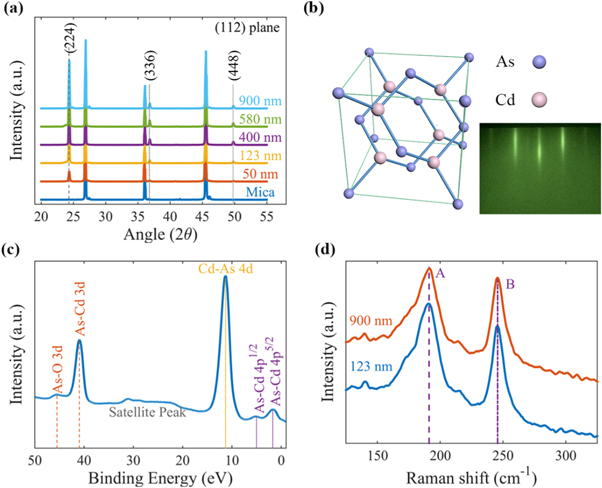
Figure 1. Characterizations of as-grown Cd3As2 thin films. (a) X-ray spectra. The marked peaks are the typical Cd3As2 (112) plane XRD patterns. Other peaks come from the mica substrate and the peak intensity increases with the thickness of Cd3As2. (b) Cd3As2 in a tetragonal body center unit cell with a = b = 12.633(3) Å and c = 25.427(7) Å. The inset figure shows the corresponding in situ RHEED pattern for the Cd3As2 thin films. (c) Typical core-level photoemission spectrum measurements for a Cd3As2 thin film, where Cd 4d, As 3d and As 3p peaks are clearly observed. The composition of Cd3As2 can be derived from the integrated area of these peaks and corresponding sensitivity factors. (d) Raman spectra for different thickness Cd3As2 thin films.
Download figure:
Standard image High-resolution imageThe Cd3As2 thin films were patterned into standard six-probe Hall bar geometry with the channel size of 1 mm × 0.5 mm, as displayed in figure 2(a). Figure 2(b) shows the temperature-dependent longitudinal magneto-resistance Rxx of the Cd3As2 thin films (Σ1 ∼ Σ5) with various thickness at zero magnetic field. It is noted that Rxx monotonically increases with the thickness d decreasing, and the Rxx-T slope at the low temperature region shows a change from positive to negative, indicating a semimetal-to-semiconductor transition. For the thickest Cd3As2 sample (Σ5, ∼900 nm), Rxx reveals a broad peak at T ∼ 225 K below which the resistance exhibits a metallic behavior that is commonly found in semimetals or gapless semiconductors. When the thickness is reduced to ∼400 nm (Σ3), the resistance increases slightly in the range of 10 to 2 K. One possible reason is that due to the zero energy gap and a low carrier density n3D ∼ 0.12 × 1018 cm−3, holes are copiously excited even at low temperatures, and the increased hole population could lead to a decrease in Rxx, similar to that observed in Na3Bi system [36]. When further reducing thickness (Σ1, 50 nm) (several thinner samples are available in supporting information figure S1), the semiconducting behavior becomes evident, consistent with the theoretical predictions, i.e., a bandgap opening when the dimensionality is reduced in Dirac semimetals [3].
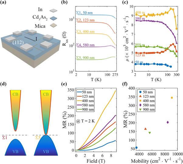
Figure 2. Thickness-dependent transport properties for Cd3As2 thin films. (a) Schematic diagram of a standard six-probe hall bar, used for the transport measurements. A magnetic field B up to 9 T was applied perpendicular to the (112) plane. (b) Temperature-dependent longitude resistance Rxx-T for the five Cd3As2 thin films at zero magnetic field, with the thickness d varying from 50 to 900 nm; Rxx drops as the sample thickness reduces, displaying a thickness-induced insulator-to-metal transition. (c) Carrier mobility μ = |RH|/ρ0 versus temperature. Here, the Hall coefficient RH was evaluated from the measurements with B = 0 ∼ 4 T. The carrier mobility is about 3750–9750 cm2 V−1 s−1 at 2 K. (d) Sketch of band structure with band gap opening for Cd3As2 thin films. (e) The SdH oscillations of longitudinal magneto-resistance at 2 K. It shows non-saturation behavior and the largest ratio reaches 343.5%. (f) A nearly linear relationship between MR and electron mobility, which drops from 343.5% to 58.8%.
Download figure:
Standard image High-resolution imageMagneto-transport measurements were carried out at low temperatures for different thickness films using a physical properties measurement system (PPMS, up to 9 T). The transverse resistance (Rxy) versus magnetic field B is measured at T = 2 K (See supporting information figure S2 for Rxy-B). The negative slope of Rxy suggests that the dominant charge carriers in Cd3As2 thin films are electrons. Figure 2(c) depicts the typical temperature-dependence of Hall mobility (μ) deriving from the Rxy - B linear parts. Most of our Cd3As2 thin films yields a high mobility in the range of 3.8 ∼ 9.1 × 103 cm2 · V−1 · s−1 at 2 K. And the mobility significantly increases as the temperature T drops. This can be attributed to the alleviated electron-phonon scattering at low temperatures. The sheet carrier density (ns) at 2 K varies between 3.4 ∼ 24 × 1012 cm−2, and the corresponding carrier concentration (n3D) is determined to be a relative low value of 1 ∼ 8 × 1017 cm−3. Figure 2(d) depicts a band schematic structure for a typical Cd3As2 thin film with an emerged gap opening when the dimensionality reduces. The Fermi levels labeled in the sketch are determined by the SdH oscillations as discussed below. The relative position between the Fermi level and the band edge is qualitatively consistent with the aforementioned Rxx-T curves. Moreover, figure 2(e) shows a large positive magneto-resistance (MR = [Rxx(B)-Rxx(0)]/Rxx(0) × 100%) at 2 K for the Cd3As2 series films with a parabolic and a quasi-linear behavior at low- and large-fields (B ≥ 5 T), respectively. It shows a linear behavior without saturation and the maximum MR ratio is closed to 343.5% at B = 9 T. Interestingly, we also find that the corresponding ratio at 9 T drops from 343.5% to 58.8% that is associated with the electron mobility. And there is a nearly linear relationship between MR and μ as shown in figure 2(f), consistent with the previous studies [12]. Owing to the Dirac band structure and the high mobility of the thin Cd3As2 films, we were able to resolve SdH oscillations in Rxx for most of our samples at low temperature (2 K), as shown in figure 2(e).
To fundamentally study the thickness-induced transition, we determined the electron mean free path using  (3π2n3D)1/3 and the 3D Fermi wave vector by kF = (3π2n3D)1/3, as summarized in table SII (See the supplementary material), where n3D is the 3D carrier density, d is the film thickness, e is the electron charge, and
  is the reduced Planck's constant. Figures 3(a), (e) and (i) present the vertically shifted SdH oscillation amplitude ΔRxx versus 1/B at different temperatures for samples Σ1, Σ4 and Σ5, respectively, after subtracting a smooth background. A clear periodic fluctuation in resistance are observed when T ≤ 50 K, and the oscillation amplitude decreases rapidly with increasing T. To understand the temperature-dependent SdH oscillations for the different thickness thin films, we obtain the oscillation frequency F from Landau fan diagrams (figures 3(b), (f) and (j)), taking the periodic maxima and minima of ΔRxx as the half integer and integer, i.e. peak and valley positions in 1/B, respectively. The slope yields a distinct frequency of F = 23.18 T, which corresponds to a periodicity of Δ(1/B) = 0.0431 T−1 for the thinnest sample (Σ1). The cross-sectional area of the Fermi surface SF can be determined from the Onsager equation F = (Φ0/2π2)SF, here Φ0 = h/2e. We note that, for 50 nm (Σ1), 580 nm (Σ4) and 900 nm (Σ5), F and SF varies in 23.18 ∼ 14.39 T and 2.21 to 1.37 × 10⁻³ Å−2 as the thickness d changes. The Fermi vector kF = 0.0266 ∼ 0.0209 Å can be extracted when assuming a circular cross-section
  For a 3D Dirac materials, the carrier density estimated from the SdH oscillations obeys the following formula [37]:
where gs is the spin degeneracy and gv is the valley degeneracy. Provided gsgv = 4 [13, 38], i.e., a small carrier concentration nSdH is calculated to vary from 1.276 to 0.618 × 1018 cm−3, which is reasonably consistent with the n3D value from the Hall effect measurements (See supporting information table SI for Hall parameters).

Figure 3. Shubnikov-de Hass Oscillations from the Cd3As2 thin film samples Σ1 (upper), Σ4 (center)and Σ5 (lower), respectively. (a), (e), (i) The vertical shifted oscillation component ΔRxx against 1/B, after subtracting a fitted smooth background at various temperatures. The ΔRxx traces are vertically shifted for clarity. (b), (f), (j) Landau fan diagrams. The blue squares denote the integer index (ΔRxx peak), and the red circles indicate the half integer index (ΔRxx valley). It can be linearly fitted, resulting in the intercept 0 < γ + δ < 1. (c, g, k) The normalized temperature-dependent SdH oscillation amplitude ΔRxx(T)/ΔRxx(0) for the first visible Landau level. The cyclotron effective mass m* can be extracted by fitting to the Lifshitz-Kosevich formula (green solid line). (d, h, l) Dingle-plot for ΔRxx oscillations Ln[(ΔRxx/R0)Bsinh ![$(2{\pi }^{2}m* {k}_{B}T/\hslash eB)]$](https://content.cld.iop.org/journals/1367-2630/18/8/083003/revision1/njpaa3293ieqn4.gif) versus 1/B at different temperature.
versus 1/B at different temperature.
Download figure:
Standard image High-resolution imageIn order to further verify the temperature-dependence of SdH oscillations and extract key carrier transport parameters, we fit the oscillation amplitude ΔRxx to the standard Lifshitz-Kosevich theory [37],
where  and
and  are the thermal factor and the Dingle factor, respectively. Here, kB is the Boltzmann's constant, m* is the cyclotron effective mass,
  is the Dingle temperature, τ is the quantum lifetime due to scattering, and 2πβ is the Berry's phase which will be discussed later.
Thus, the normalized oscillation amplitude can be described as ΔRxx(T)/ΔRxx(0) = λ(T)/sinh(λ(T)). We plot the ΔRxx(T)/ΔRxx(0) for sample Σ1, Σ4 and Σ5 in figures 3(c), (g) and (k), based on which the effective mass m* are extracted to be 0.0322 ∼ 0.0254 me (me is the free electron mass). By employing  and
and  we can obtain the Fermi velocity νF = 11.0 ∼ 9.53 × 10⁵ m s−1 and the Fermi energy EF = 193.2 ∼ 131.2 meV. The Dingle-plot for SdH oscillations ln[(ΔRxx/R0) · B · sinh
 ![$(2{\pi }^{2}m* {k}_{B}T/\hslash eB)]$](https://content.cld.iop.org/journals/1367-2630/18/8/083003/revision1/njpaa3293ieqn10.gif) versus 1/B and the linear fitting curves at different temperatures are shown in figures 3(d), (h) and (l). All these estimated parameters derived from the SdH oscillations at T = 2 K are provided in table 1.
versus 1/B and the linear fitting curves at different temperatures are shown in figures 3(d), (h) and (l). All these estimated parameters derived from the SdH oscillations at T = 2 K are provided in table 1.
Table 1. Estimated parameters from the SdH oscillations at T = 2 K for Σ1, Σ4 and Σ5 Cd3As2 samples.
| d | F | SF | kF | nSdH | m* | vF | EF | |
|---|---|---|---|---|---|---|---|---|
| nm | T | γ + δ | 10−3 Å−2 | Å−1 | 1018 cm−3 | me | 105 m s−1 | meV |
| 50 | 23.18 ± 0.05 | 0.325 ± 0.010 | 2.21 ± 0.004 | 0.0265 ± 0.0012 | 1.262 ± 0.012 | 0.322 ± 0.0016 | 9.54 ± 0.64 | 166.6 ± 17.7 |
| 580 | 23.35 ± 0.35 | 0.657 ± 0.055 | 2.23 ± 0.03 | 0.0266 ± 0.0032 | 1.276 ± 0.024 | 0.0280 ± 0.0009 | 11.0 ± 1.40 | 193.2 ± 35.3 |
| 900 | 14.39 ± 0.22 | 0.741 ± 0.043 | 1.37 ± 0.02 | 0.0209 ± 0.0026 | 0.618 ± 0.012 | 0.0254 ± 0.0012 | 9,53 ± 1.25 | 131.2 ± 23.6 |
To further clarify thickness-dependent SdH oscillations, Berry's phase has been obtained from the Landau fan diagram as shown in figures 3(b), (f) and (j). According to the Lifshitz-Onsager quantization rule [39]:
The Berry's phase 2πβ can be extracted from the intercept in Landau fan diagram by γ + δ, 2πδ is an additional phase shift determined by dimensionality, which equal to 0 for a quasi-2D cylindrical Fermi surface and ±π/4 (+ for holes and—for electrons) for a corrugated 3D Fermi surface. For nontrivial π Berry's phase observed in bulk Cd3As2 [14] as reported before, γ should be 1. In our experiments for the different thickness Cd3As2 thin films, the intercepts γ + δ are about 0.325 ∼ 0.741 and the corresponding Berry phase 2πβ are about −0.099π ∼ 0.732π. And it shows a tendency that the Berry phase changes from zero to π Berry's phase as the thickness increases, i.e. Cd3As2 exhibits a transition from trivial band insulator to nontrivial Dirac semimetal as the dimensionality increases from quasi-2D thin film to 3D bulk, which is consistent with theoretical predictions [3]. The presence of zero Berry's phase for the thinnest Cd3As2 sample (Σ1) infers that the SdH oscillations mainly drive from the high mobility bulk conduction band, and the Dirac point vanishes along with the band gap opening as the dimensionality reduces, which also agrees well with the thickness-dependent Rxx-T results as discussed previously.
For a nontrivial π Berry phase, the offset γ + δ in the LL fan diagram should be 1. Here, the Fermi surface's curvature can generally lead to a 1/8 intercept shift [39]. But for our thickest film (Σ5, figure 3(j)), the LL fan diagram intercept 0.741 is close to γ -1/8 (γ = 1), approaching the non-trivial Berry's Phase. It might be because the Fermi surface SF is still an anisotropic ellipsoid instead of a perfect sphere. On the other hand, in previous study [40], when the magnetic field B is perpendicular to (112) plane, the large field can break the crystal symmetry. A gap may subsequently emerge as long as the orbit-coupled field strength is smaller than the mass term, which could further cause an extra phase shift. However, we speculate that this effect is fairly weak in the range of 0–9 T although it may still have some effect.
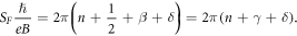
We further performed angular-dependent magneto-transport measurements for the Cd3As2 thin films and obtained the vertically shifted SdH oscillations amplitude ΔRxx against angle θ after removing the background signals. Here, θ is the angle between magnetic field B and (112) plane normal direction, varies from 0° to 90° correspond to the changing from out-plane to in-plane. And we note that the oscillations frequency F at different angles θ, which is related to the cross-sectional area of the Fermi surface SF in the momentum space, can be used to estimate the configuration of the Fermi ellipsoid via the Onsager equation. The variation of F reduces and it remains almost unchanged (within 2%) for the thickest film (Σ5, 900) as θ varies from 0° to 90°, as shown in figure 5. This small anisotropy points to a nearly uniform Fermi ellipsoid surface in kx and ky direction for Cd3As2 thick films, which is qualitatively consistent with the recent magnetron-transport experiment results [14, 40, 41]. But for thinner films (Σ1, as shown in figure 4(a)) ΔRxx starts to decrease when θ goes beyond 45° and the peak nearly vanishes at θ = 90°. It may be explained as (due to the quantum confinement in the normal direction [112]) the ellipsoids Fermi surface were evaluated into anisotropic ellipsoids Fermi surface as the dimensional reduced.
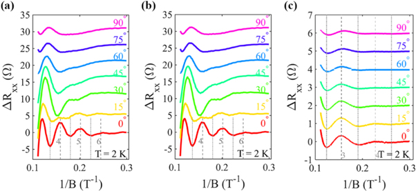
Figure 4. Angular-dependent SdH oscillations from the Cd3As2 thin films Σ1 (left), Σ4 (center)and Σ5 (right) measured at T = 2 K, respectively. (a), (b), (c) The SdH oscillation amplitude ΔRxx venues 1/B (after subtracting a smooth background) at various tilted angle θ.
Download figure:
Standard image High-resolution image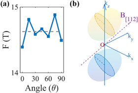
Figure 5. Fermi surface parameters from the thickest Cd3As2 thin films (Σ5). (a) The oscillation frequency F as a function of θ deduced from the Landau fan diagrams. (b) A schematic Fermi surface for 900 nm-thick thin film.
Download figure:
Standard image High-resolution image
In conclusion, we have produced single-crystalline Cd3As2 thin films with different thickness (50 ∼ 900 nm) by MBE on the cleaved mica substrates. The corresponding crystal quality and thin film properties were characterized by XRD, XPS and Raman measurements. We found a dimensionality-induced semimetal-to-semiconductor transition and Rxx shows semiconducting behavior owing to an emerged band gap opening for the thinnest film (50 nm). Furthermore, the temperature-dependent SdH oscillations are observed, suggesting non-trivial to trivial Berry's phase transition.
Acknowledgments
This work was supported by the National Young 1000 Talent Plan, National Natural Science Foundation of China (61322407, 61376093, 11474058). F X Xiu acknowledges the open project from National Laboratory of Solid State Microstructures, Nanjing University (project #M29020). F Q Song acknowledges the open project from State Key Laboratory of Surface Physics and Department of Physics, Fudan University (project #KF2016_04).
Competing financial interests
The authors declare no competing financial interests.