


Abstract
Kitaev's 0–π qubit encodes quantum information in two protected, near-degenerate states of a superconducting quantum circuit. In a recent work, we have shown that the coherence times of a realistic 0–π device can surpass that of today's best superconducting qubits (Groszkowski et al 2018 New J. Phys. 20 043053). Here we address controllability of the 0–π qubit. Specifically, we investigate the potential for dispersive control and readout, and introduce a new, fast and high-fidelity single-qubit gate that can interpolate smoothly between logical X and Z. We characterize the action of this gate using a multi-level treatment of the device, and analyze the impact of circuit-element disorder and deviations in control and circuit parameters from their optimal values. Furthermore, we propose a cooling scheme to decrease the photon shot-noise dephasing rate, which we previously found to limit the coherence times of 0–π devices within reach of current experiments. Using this approach, we predict coherence time enhancements between one and three orders of magnitude, depending on parameter regime.
Export citation and abstract BibTeX RIS

Original content from this work may be used under the terms of the Creative Commons Attribution 3.0 licence. Any further distribution of this work must maintain attribution to the author(s) and the title of the work, journal citation and DOI.
1. Introduction
Fault-tolerant quantum computation is likely to require daunting hardware resources [1, 2]. This fact motivates the search for strategies to reduce the qubit overhead needed for quantum error correction, and drives the development of new quantum error correcting codes [3–7]. Furthermore, the reduction of gate errors for physical qubits offers a direct and impactful way of reducing qubit overhead [2, 8]. The latter can be achieved both through longer qubit coherence times and better quantum control for gates.
For superconducting circuits, coherence time improvements by as much as five orders of magnitude have been demonstrated [9, 10]. This has been possible thanks to advances in several areas, including materials [11], microwave engineering [12], shielding [13, 14], and the use of 3D architectures [15–17]. Crucially, order-of-magnitude leaps in coherence have also been the result of new qubit designs, such as the transmon and the fluxonium qubits [18, 19].
In this paper, we consider the superconducting circuit introduced in [20], commonly referred to as the 0–π qubit, and closely related to Kitaev's current mirror proposal [21]. With a set of non-overlapping logical wave functions and very low flux and charge dispersion, the 0–π qubit displays exponential suppression of relaxation and dephasing. It has been shown that the 0–π qubit can be used to encode quantum information in a protected subspace [20–23], but in a regime of parameters that is challenging to realize with current superconducting quantum circuits. In fact, the fully protected regime of this device exploits a degree of freedom with large quantum fluctuations, something which requires an effective impedance surpassing the quantum of resistance by orders of magnitude. Achieving this regime requires the use of superinductors, which are circuit elements with inductance greater than ∼100 nH and with very little stray or ground capacitances [19, 24–26]. We have recently shown that for circuit parameters attainable with current superconducting technology, the 0–π qubit dephasing time is limited by photon shot noise arising from a parasitic circuit mode (which we referred to as the ζ-mode) [22]. Nevertheless, we found that the 0–π qubit still has the potential to outperform state-of-the-art superconducting devices. Below, we propose a method to further enhance the coherence time by orders of magnitude by cooling the ζ-mode.
However, as can be expected, the price of intrinsic noise protection in the 0–π qubit is that it is difficult to perform logical operations on this device. In particular, protection from noise comes in part from the exponentially small overlap of its logical wave functions. As a result, matrix elements of local operators between the two logical states will also be small, thus resulting in extremely slow gates. In [20], Brooks et al proposed a universal set of protected logical operations based on coupling to an ultra-high impedance LC oscillator. However, these operations were based on an idealized model of the qubit and with parameters that are difficult to realize in practice. Further work is required to determine the potential of this approach in a more realistic setting.
Motivated by the prospect of realizing 0–π qubits in the near term, we investigate alternative approaches to measurement and control with lower experimental complexity. The operations we propose are not protected in the same sense as those proposed in [20], because they rely either on operating the device in a regime where the qubit is not fully isolated from the environment, or they make use of excited states outside the qubit manifold. In particular, we develop a single-qubit gate based on a multi-level excursion through higher energy levels. Nevertheless, we hope that these schemes will be useful for both characterization and control of 0–π qubits in near-to-medium-term experiments.
This work is organized as follows. In section 2, we introduce the 0–π qubit and provide a simplified effective model for the 0–π circuit with only a single degree of freedom. In section 3, we discuss general coupling strategies for qubit control and readout, and derive the 0–π circuit Hamiltonian accounting for stray and parasitic capacitances, disorder in circuit-element parameters, as well as coupling to microwave voltage sources and a readout resonator. In section 4, we analyze dispersive coupling to a resonator, and find that there are regimes of dispersive shift akin to the straddling regime of the transmon qubit [18]. In section 5, we introduce a single-qubit gate that achieves population inversion of the 0–π qubit and can interpolate between logical X and Z by varying the qubit operation point. Furthermore, we characterize the gate operation as a function of circuit design parameters and analyze its robustness. In section 6, we propose a method to fight the main qubit dephasing mechanism, analyze its performance as a function of circuit parameters, and discuss its implementation. We conclude in section 7.
2. The 0–π qubit in a nutshell
In this section we introduce the 0–π qubit in the ideal case of no circuit-element disorder and briefly discuss its properties. In particular, we give an intuitive picture in terms of co-tunneling of Cooper pairs leading to an approximately π-periodic qubit potential, which is further verified by an effective model accurately describing the low-energy physics of the system.
2.1. The circuit Hamiltonian
We first consider the symmetric 0–π circuit, as illustrated in figure 1(a), consisting of two Josephson junctions with energy EJ, capacitance CJ and plasma frequency  , two superinductors with inductance L, and two large capacitors with capacitance C. The normal modes of this circuit are

where φi is the superconducting phase operator at node i of the circuit. Using these definitions, the symmetric 0–π qubit Hamiltonian reads [23]

where qϕ = 2enϕ and qθ = 2enθ are the conjugate charge operators associated with ϕ and θ (i.e. [ϕ, nϕ] = i and [nθ, eiθ] = eiθ) respectively, and φext = Φext/φ0 is the external magnetic flux in units of the reduced flux quantum φ0 = ℏ/2e. Moreover, we have introduced capacitances for the two qubit modes ϕ and θ given by Cϕ = 2CJ and Cθ = 2(C + CJ), respectively, and the inductive energy  .
.

Figure 1. The 0–π qubit in a nutshell. (a) Circuit diagram for the symmetric 0–π qubit, with pairwise identical circuit elements. (b) Pictorial illustration of co-tunneling of pairs of Cooper pairs across the two junctions, explaining the approximate π-periodic potential energy, and an equivalent circuit-element with only a single degree of freedom θ.
Download figure:
Standard image High-resolution imageIn the 0–π qubit, quantum information is stored in the {ϕ, θ} degrees of freedom, while ζ is a spurious low-frequency harmonic mode and Σ is a cyclic coordinate. In absence of circuit-element disorder, the ζ and Σ modes do not couple to ϕ and θ, and are therefore excluded from equation (2).
Introducing the effective impedances  and
and  , where
  the 0–π regime is defined by

where RQ = h/(2e)2 ≃ 6.5 kΩ is the superconducting quantum of resistance. We say that a device is in the 'moderate,' or 'deep' 0–π regime, depending on the degree to which the impedance relations are satisfied. The problem of fabricating a qubit in the deep 0–π regime, includes that of realizing a high-impedance superinductor [27–29].
2.2. Exciton tunneling picture
Figure 1(b) shows an approximate equivalence between the 0–π circuit (to the left) and a circuit-element describing tunneling of pairs of Cooper pairs (to the right). The co-tunneling of Cooper pairs or 'exciton' in the 0–π circuit can be understood as a consequence of a circuit layout combining branches of superinductors (high impedance) and large capacitances (low impedance). Here, we schematically illustrate how tunneling of a Cooper-pair across the left junction of the 0–π circuit is 'mirrored' by the simultaneous tunneling of a Cooper-pair across the right junction: a Cooper-pair tunneling event across the left junction leads to a build up of −2e negative charge on one side of one of the large capacitors, which must be compensated for by a positive charge on the other side. This can happen through a simultaneous −2e Cooper-pair tunneling event across the right junction in the same direction. The co-tunneling of Cooper pairs through the left and right junctions form together an effective exciton tunneling event [21].
Note that no current flows through the superinductors in the limit of  (
( ). Superinductors are, however, crucial in defining the non-trivial topology of the circuit, as in their presence we can identify two distinct circuit islands shown as blue (bottom) and pink (top) in figure 1(b). Due to the simultaneous co-tunneling of Cooper pairs across the two junctions, we expect the potential energy to be π-periodic rather than 2π-periodic in the superconducting phase difference across the two islands, in the limit
  . This expectation can be verified by an effective model for the θ degree of freedom alone, derived in appendix B following a Born–Oppenheimer approach and resulting in the effective Hamiltonian

where  and
and  are, respectively, the charging energy and the offset charge corresponding to the θ coordinate. The flux-dependence of the potential energy is given by the coefficients
  and
and  , where Eα, Eβ and Eγ are constants dependent on the qubit design parameters and studied below.
In the moderate-to-deep 0–π regime, the relations  and
and  are satisfied. The effective one-dimensional potential in equation (4) is shown in figure 2(a) for a set of 0–π circuit parameters. As a function of flux, the two nearly degenerate minima are detuned one with respect to the other, except at φext = π, where the potential becomes perfectly π-periodic. With
  , tunneling between the two wells is highly suppressed. In the presence of a small, positive E1 (−π < φext < π), the lowest-energy state is localized in θ = 0 and a nearly degenerate first excited state is localized in θ = π. At φext = π, the two minima at θ = 0 and θ = π are exactly degenerate and the logical wave functions become hybridized independently of the circuit design parameters. For E1 smaller than or comparable to the tunneling rate between the potential wells, hybridization can also occur at
  .
.

Figure 2. (a) Effective one-dimensional potential (black) and wave functions for the two lowest lying energy states (color), extracted using a Born–Oppenheimer approach (see appendix B). To the right of the effective potential we show a schematic of the energy diagram (not to scale). In the moderate-to-deep 0–π regime, the low-energy spectrum consists of nearly degenerate doublets in a weakly anharmonic ladder, closely resembling a transmon qubit spectrum with each transmon level replaced by a doublet. The two lowest doublets are split by approximately  , corresponding to the plasma frequency of the π-periodic Josephson element. (b) Energy parameters of the one-dimensional Hamiltonian equation (4) as a function of Zϕ for fixed Zθ. We observe an exponential suppression of both Eβ and Eγ, indicating that the qubit becomes a flux-insensitive π-periodic Josephson element in the deep 0–π regime. Eα remains almost unchanged in comparison. Circuit parameters: EL/ℏωp ∈ [1.25 × 10⁻⁴, 5 × 10⁻³] and
  .
.
Download figure:
Standard image High-resolution imageFigure 2(b) shows the values of {Eα, Eβ, Eγ} obtained from a numerical calculation of the coefficients in equation (4) as a function of Zϕ/RQ for fixed Zθ (see appendix B for details). We observe an exponential suppression of the  potential term relative to the
  term, justifying the π-periodicity suggested by the intuitive picture of co-tunneling of Cooper pairs. We note that the effective Hamiltonian equation (4) in the limit E1 = 0 resembles that of a transmon qubit, with the crucial distinction that the two minima at θ = 0 and θ = π are physically distinct. We also note, as shown in the inset in figure 2(b), that E2 ≃ Eα ∼ EJ. The condition
  thus translates to
  , or equivalently
  .
.
Based on this simple picture, the 0–π qubit approximately reduces to a device with one effective degree of freedom, θ, whose conjugate charge operator, nθ, determines the Cooper-pair number difference between the two circuit islands identified in figure 1(b). Since nθ changes in units of two, Cooper-pair parity is a conserved quantity and an approximate symmetry of the circuit Hamiltonian. We emphasize that the symmetry is approximate, since for finite Zϕ, the  term in equation (4) breaks the symmetry.
2.3. Qualitative explanation of robustness to noise
Cooper-pair parity conservation partitions the qubit spectrum into doublets with exponentially small charge sensitivity in the 'transmon limit'  [18, 30]. The π-periodicity of the Hamiltonian moreover allows us to draw several qualitative conclusions about the qubit's generic properties. Formally, we define a symmetry operator
  which displaces θ by π, and note that

where the ellipses refer to exponentially small corrections in the deep 0–π regime, as we have verified above. Denoting the ground state of the Hamiltonian by  with energy E0, it follows that a second eigenstate with energy exponentially close to E0 is given approximately by
  . This follows from
  We can denote this eigenstate by
  . Moreover, the argument continues to hold in the presence of any perturbation to the Hamiltonian that respects the (approximate) symmetry equation (5), i.e.

where V satisfies  It follows that dephasing noise is expected to be exponentially suppressed for symmetry-preserving noise processes. In particular, equation (4) shows that external flux noise does not break the π-periodicity [recall that E1(φext) is exponentially suppressed in the deep 0–π regime].
The condition  (or equivalently
  ) moreover leads to exponential suppression of tunneling between the two potential wells located at θ = 0 and θ = π, as already discussed. When the two nearly degenerate ground states are localized in the two different wells, this thus leads to an exponential suppression of bit-flips6

for V any weak perturbation to the Hamiltonian that is local in phase space, i.e. any low-degree polynomials in {ϕ, θ, qϕ, qθ}. Equations (6), (7) lead together to the remarkably long coherence times expected for the qubit in the deep 0–π regime, as recently confirmed quantitatively in [22].
3. Coupling to external circuitry
3.1. General remarks about coupling strategies
With the goal of controlling and measuring the 0–π qubit, we now outline different strategies to couple the qubit to external degrees of freedom. Noise protection in the 0–π qubit is achieved at a high price: the protection from bit-flips implies negligible matrix elements for qubit transitions making many coupling schemes inefficient. Moreover, great care has to be taken to not introduce coupling circuitry explicitly breaking the π-periodicity, opening the qubit to dephasing noise. Some general remarks about coupling strategies can be made based on the qualitative discussion of the 0–π qubit in the previous section.
3.1.1. Direct inductive coupling
Any galvanic linear inductive coupling to the four circuit nodes leads to contributions of the generic form  to the Hamiltonian, explicitly breaking the 0–π periodicity and lifting the groundspace degeneracy. It might be possible to approximately restore the 0–π periodicity by using superinductors such that EL,θ → 0. However, this in turn leads to negligible coupling to any external circuitry, rendering such an approach ineffective.
3.1.2. Mutual inductive coupling
As mentioned above, in the limit  , moderate variations of the external flux through the qubit loop do not break the 0–π symmetry, such that mutual inductive coupling can potentially be a symmetry-preserving coupling mechanism. However, for precisely the same reason that the qubit is highly insensitive to flux noise [22], control and readout strategies based on mutual inductive coupling are ineffective. Large external flux excursions, in contrast, can be used to move between regimes where the logical states are localized in different potential wells, to a regime where they are in a superposition of both wells. We discuss exploiting this in a control strategy in section 5.
3.1.3. Capacitive coupling
Capacitive coupling to the circuit nodes has the advantage that it only couples directly to the charge degrees of freedom, leaving the 0–π periodicity and the two-island topology in figure 1(b) intact. Moreover, as long as the coupling capacitances are kept small, they should not compromise the inequality equation (3). In general, the extremely small matrix elements coupling the logical qubit states make many conventional control and readout strategies inefficient. Nevertheless, we show below that capacitive coupling can be used to perform device spectroscopy in a moderate-to-deep regime of parameters, enable single-qubit control by means of fast voltage drives, and cool the parasitic ζ-mode to improve the qubit coherence times.
3.1.4. Nonlinear symmetry-preserving inductive coupling
Although we have argued that any straightforward coupling strategy based on inductive elements is either ineffective or breaks the qubit's protection from noise, it might still be possible to engineer nonlinear inductive couplers that respects the 0–π symmetry. This means that the inductive contribution to the energy has to satisfy Ecoupler(θ) = Ecoupler(θ + π) + ..., where the ellipses again refer to terms that vanish in the deep 0–π regime. In [20], it was proposed that such a coupling mechanism can be achieved by using a tunable Josephson coupler (SQUID loop) connecting the 0–π qubit to an LC oscillator. For the qubit to remain protected, the LC oscillator with impedance Zr is required to satisfy  , much like the internal ϕ mode of the 0–π circuit. Moreover, it was shown that such a coupling could be used to enact one- and two-qubit phase gates. We briefly return to this scheme below, and point out some additional challenges which have previously been overlooked.
3.2. Addressing the 0–π qubit degree of freedom
Coupling to the qubit mode θ in the 0–π circuit has an additional challenge, beyond the general points already made above. Because the coordinate θ is a combination of phase operators of all nodes of the circuit [see equation (1)], addressing only this coordinate requires a coupling element acting symmetrically on both ports of each superinductor. As illustrated schematically in figure 3(a), where the boxes represent unspecified coupling elements and could be capacitive or inductive in general, this coupling circuitry necessarily shunts the 0–π qubit superinductors. According to the discussion in section 2.2, if the impedance of the coupler is not greater than or comparable to that of the qubit superinductors, this effect can potentially compromise regime of operation of the device. At first glance, a possible solution to this problem appears to be the use of additional superinductors replacing each of the box-shaped couplers in figure 3(a). However, this would lead to an inductive shunt of the 0–π circuit islands identified in figure 1(b) through the readout or control circuit [represented by a meter in figure 3(a)], breaking the Cooper-pair parity symmetry.

Figure 3. (a) Addressing the qubit main degree of freedom θ. The small box-shaped couplers are used to represent arbitrary coupling circuit elements, and the meter represents a readout or control circuit. As illustrated by a dashed frame, the required coupling circuitry (in red) necessarily shunts the device superinductors, leading to a combined link impedance Z(ω) that can compromise the qubit operation. (b) Coupling layout originally considered in [20]. The interaction strength J(t) stands for the potential energy of a flux-tunable device.
Download figure:
Standard image High-resolution imageAn alternative coupling scheme considered in [20] is illustrated in figure 3(b). In this scheme, the coupling element (i.e. the box in the figure) is a SQUID loop giving a tunable Josephson element between the 0–π circuit and the LC oscillator. This coupling layout overcomes the difficulty described at the beginning of this section by relaxing the symmetry requirements of the coupling circuitry. However, this leads to an interaction Hamiltonian that involves both θ and the spurious ζ-mode

where J(t) is the tunable Josephson-energy of the coupling element, and ϕr the resonator phase operator. We have previously shown that the ζ-mode frequency goes to zero in the deep 0–π regime leading to diverging thermal occupation of this mode [22], something which was not taken into account in [20]. The impact of thermal fluctuations due to the 0–π circuit internal modes thus requires further study and we propose in section 6 a cooling scheme that can help approximate the ideal behavior considered in [20].
Based on this discussion, the most viable option for near-term experiments appears to be the use of capacitive coupling. This means replacing the box-shaped couplers in figure 3(a) by capacitors. Formally, small coupling capacitors operate as high-impedance links while preserving the circuit islands. The coupling capacitances must be kept small to ensure  since these add to Cϕ [see equation (A.1)]. Therefore, a downside of this approach resides in the fact that the capacitive couplings cannot be very large. Nevertheless, we find that capacitive coupling allows for significant dispersive shifts (section 4), and a fast, single-qubit gate (section 5).
We emphasize that the control strategies we consider in the following are not fault-tolerant in the sense of [20, 21]. They either rely on operating the qubit in a regime that is not fully protected, or involve populating higher and less robust excited states. Nevertheless, these operations can be performed with high-fidelity and are thus suitable for implementation in realistic devices in the near future.
3.3. Capacitive coupling to voltage sources
We now consider the 0–π circuit in the presence of voltage sources Vi connected to the nodes i = 1, ..., 4 of the circuit, as shown in figure 4(a). Since we have found that circuit-element disorder is a limiting factor for the qubit coherence for parameters within reach of current experiments [22], we include such effects here. In particular, we account for any superinductance and Josephson-energy asymmetries, denoted by dEL and dEJ, respectively, as well as capacitance asymmetries, denoted by dCJ and dC. Additionally, there can be disorder in the gate capacitances ( ), as well as in the parasitic capacitances to ground (
 ), such that the node gate and ground capacitances for node i are
  and
and  respectively. We note that, in practice, the stray capacitances may arise from the superinductances and the large capacitors of the 0–π circuit [28]. Following the standard approach to circuit quantization [31, 32] we find the Hamiltonian

where  describes the un-driven qubit. The first contribution

with qμ/2e = −i∂μ for μ = (ϕ, θ, ζ, Σ) is the ideal 0–π Hamiltonian, where we now explicitly include the ζ and Σ degrees of freedom and the mode capacitances Cμ defined explicitly in appendix A. On the other hand,

describe unwanted spurious couplings between the circuit modes to leading order in circuit-element disorder. The last term  is a purely capacitive term accounting for disorder of the gate and ground capacitances, and its full expression can be found in appendix A. Since these capacitances are expected to be much smaller than the internal circuit capacitances C, we however neglect
  in the remainder of this work. Finally, the drive term

describe voltage drives of the four normal modes where Vμ is defined in terms of the node voltages Vi with i = 1, ..., 4 according to the transformation rule in equation (1). Circuit-element disorder furthermore introduces additional drive terms. This is accounted for by the Hamiltonian  , given explicitly in appendix A.

Figure 4. (a) Lumped-element model for the 0–π circuit coupled to microwave voltage sources, including gate and ground capacitances for each circuit node. (b) 0–π circuit connected to a resonator with nodes p1 and p2. The shown coupling layout couples the resonator charge operator to qθ, and corresponds to the second row in table 1.
Download figure:
Standard image High-resolution imageAs can be seen from equation (11) the coupling between the qubit degrees of freedom {ϕ, θ} and the spurious ζ-mode appears when the large circuit capacitors or the superinductors are not symmetrical:  or
or  respectively. As we have shown recently [22], this leads to the limiting contribution to the qubit's coherence time for realistic parameters due to photon shot noise for the ζ-mode. We return to how to alleviate this issue in section 6.
3.4. Capacitive coupling the 0–π qubit to a microwave resonator
With the goal of controlling and reading out the 0–π qubit, we consider its capacitive coupling to a microwave resonator as illustrated in figure 4(b). The Hamiltonian of the combined qubit-resonator system can be obtained from equation (9), by adding the free resonator Hamiltonian,  , and letting Vμ correspond to the resonator voltage7
. Table 1 specifies the replacement rules for the voltages Vμ in equation (9) that produce the qubit-resonator interaction Hamiltonian. Three possible coupling layouts addressing the 0–π degrees of freedom θ [shown in figure 4(b)], ϕ and ζ are considered. These capacitive coupling schemes are employed in section 4 for dispersive readout strategies, in section 5 to drive qubit transitions via multiple excited levels, and in section 6 to cool the low-frequency ζ-mode as a strategy to enhance the qubit coherence times.
, and letting Vμ correspond to the resonator voltage7
. Table 1 specifies the replacement rules for the voltages Vμ in equation (9) that produce the qubit-resonator interaction Hamiltonian. Three possible coupling layouts addressing the 0–π degrees of freedom θ [shown in figure 4(b)], ϕ and ζ are considered. These capacitive coupling schemes are employed in section 4 for dispersive readout strategies, in section 5 to drive qubit transitions via multiple excited levels, and in section 6 to cool the low-frequency ζ-mode as a strategy to enhance the qubit coherence times.
4. Dispersive readout
The transmon-like structure of the 0–π energy spectrum illustrated in figure 1(d) suggests that we might exploit known techniques for dispersive readout and control for transmon qubits [18]. The strong symmetry between the two potential wells at θ = 0 and θ = π, however, means that each 'transmon level' is split into a doublet, leading to important differences in dispersive coupling for a 0–π qubit as compared to a conventional transmon.
Dispersive coupling to a resonator relies on having unequal qubit-dependent dispersive shifts of the resonator frequency for the two logical states  and
and  . We compute the dispersive shifts numerically, assuming capacitive coupling between either of the two 0–π modes {θ, ϕ} and a readout resonator of frequency ωr/2π (see table 1). Denoting by ar the annihilation operator of the readout resonator and including M qubit levels, the qubit-resonator Hamiltonian can be written as

where  ,
,  and μ = {θ, ϕ}. Note that the resonator drive has not been explicitly included in equation (13). In the dispersive regime defined by
  , where Δij = (ωi − ωj) − ωr and
  is the mean number of photons in the resonator, the above Hamiltonian takes the form [33]

where the dispersive shift of the ith qubit level is given by  , with
  , and
, and  is the corresponding Lamb-shift. The second line in equation (14) is a two-level truncation where we have defined
  ,
,  ,
,  and
and  .
.
We investigate the dispersive coupling χμ as a function of the 0–π design parameters. We choose the resonator frequency such that χμ is maximized while ensuring the validity of the dispersive approximation. For the case of coupling to θ, we observe that χθ is heavily attenuated in the parameter space corresponding to a moderate-to-deep 0–π qubit regime. This is due to the fact that, in contrast to a transmon qubit, the strong symmetry between the left and right potential wells of the 0–π qubit leads to vanishing dispersive coupling to the resonator for most parameters. Moreover, since the external flux does not break this symmetry [see equation (4)], χθ can only slightly change by flux excursions.
Quite surprisingly, however, we find a significant dispersive shift for the coupling operator nϕ, as shown in figure 5. This behavior is qualitatively reminiscent to what is known as the straddling regime for the transmon qubit, in which the dispersive shift can increase by orders of magnitude [18]. Note, however, that the narrow straddling-like regime indicated in figure 5 is related to the splitting of doublets rather than the plasma-frequency separation between two sets of doublets, and the large number of qubit levels involved makes the situation more complex than in a transmon. Interestingly, the value of χϕ adds a significant contribution from qubit levels generated by excitations of the ϕ degree of freedom, which are not captured by the effective model in section 2.2.

Figure 5. Dispersive shift for the ground state doublet of the 0–π qubit as a function of the readout resonator frequency ωr/2π. The qubit spectrum is shown in black dashed lines. Note that many of such lines are superimposed due to the doublet structure of the qubit spectrum, and in particular for the ground state doublet around 0 GHz. For ϕ coupling, we observe a remarkable increase of the dispersive shift in the highlighted region, reminiscent of the straddling regime of a transmon qubit. Here the qubit design parameters correspond to a moderate-to-deep 0–π regime at φext = 0, with ( ,
,  ,
,  ) = (
) = ( ,
,  ). Furthermore, we assume Cg/Cμ = 0.2.
Download figure:
Standard image High-resolution imageIn practice, we find that the absolute value of χϕ/2π does not increase beyond a few hundred kHz in a moderate-to-deep 0–π parameter regime. This would lead to rather slow readout and resonator-mediated gates as compared to those for the transmon qubit [34, 35]. However, an appreciable χϕ could be useful to resolve the qubit nearly degenerate doublet by means of spectroscopy, and thus play an important role for device characterization. Moreover, we emphasize that the example parameter set in figure 5 is rather deep in the 0–π regime, where qubit lifetimes are predicted to be extremely long [22]. Reduced gate and and readout times might therefore be an acceptable compromise.
5. Single-qubit control through multilevel excursions
5.1. Qualitative picture
In this section, we study a process achieving population inversion between the logical qubit states. Such an operation seems challenging at first, given that, by design, the off-diagonal matrix elements of charge and phase operators in the qubit subspace are exponentially small in the deep 0–π regime [22, 23]. In particular, transition matrix elements for the charge operator can easily be 10−8 times smaller than those for the transmon qubit. We overcome this situation by exploiting the multilevel structure of the device for gate operations.
A first possible approach to circumvent the small overlap between logical states relies on Raman transitions, with the advantage of only virtually populating states outside of the protected subspace. However, in appendix C, we show that due to destructive interference the amplitudes of Raman processes in general vanish as the system approaches the deep 0–π limit. For this reason, we consider instead a gate scheme that temporarily populates excited states during the gate [36]. The gate lifts some of the qubit's protection from noise, as it populates higher energy levels. Nevertheless, the proposed strategy requires leaving the qubit subspace only for very short times, and we consequently find high fidelities for a broad range of parameters.
An intuitive understanding of the proposed gate can be gained by returning to the effective one-dimensional model for the 0–π qubit presented in section 2.2. In this simplified scenario, we have already suggested that logical  can approximately be obtained from
  using a displacement by π along θ. Such an operation corresponds to the unitary
  , which can be generated by voltage driving the qubit. The precise logical action of such a displacement, however, depends on circuit and external parameters, as this determines the structure of the logical wave functions in the two wells. Figure 6 shows the logical wave functions corresponding to three different points in parameter space that will be studied in detail below. The figure shows the logical wave functions before and after a shift of θ → θ + π that represents the gate operation. When ground and excited states are respectively localized in the θ = 0 and θ = π wells of the 0–π qubit potential (figure 6(a)), a π-shift corresponds to a Pauli X operation. If
  is lowered, the hybridization of the qubit logical states increases. In the situation illustrated in figure 6(b), the logical wave functions are no longer perfectly localized and the gate implements a Hadamard operation. If, instead, the logical wave functions are completely hybridized (figure 6(c)), a π-shift corresponds to a Pauli Z gate. We can alternatively achieve the same wave function control by varying the external flux where φext = 0 corresponds to localized wave functions (for large
  ) and φext = π to completely hybridized wave functions. In the following sections we study this qualitative picture in detail.

Figure 6. Single-qubit gate operation within the effective 0–π model for three chosen configurations: (a)–(c) correspond (respectively from top to bottom) to the qubit parameters highlighted with light-blue dots in figure 7(b). Ground (in blue) and excited (in orange) wave functions are displayed on the top- and bottom-left corner of each panel, respectively. To the right of the panels, we show the effect of a π-shift on such wave functions, demonstrating the gate operation. Note that because of the 2π-periodicity of the 0–π potential (in black), a π-shift to the left is equivalent to a a π-shift to the right. The gate implements a Pauli X operation for the case (a), a Hadamard for (b), and a Pauli Z for (c).
Download figure:
Standard image High-resolution image5.2. Gate fidelity with respect to circuit parameters
When the full 0–π Hamiltonian is considered, the asymmetry of the two-dimensional logical wave functions along the ϕ-direction (see figure B1(c)) make clear that  and
and  cannot be simply exchanged by means of a θ-translation alone. Taking this into consideration, this section studies the gate employing the full circuit Hamiltonian equation (9). We characterize the gate fidelity as a function of the 0–π design parameters, and analyze the effect of circuit-element disorder and pulse shaping in the following sections.
We first consider a square microwave voltage pulse applied to the qubit and driving the θ coordinate, in absence of circuit-element disorder. In equation (9), this situation corresponds to setting all Vμ to zero with the exception of Vθ, such that the circuit Hamiltonian reads

In this section, we assume that the microwave drive is turned on at t = 0, reaching an amplitude Vsq for a period of time tg. The effect of pulse shaping is analyzed below. To determine the optimal drive strength given the 0–π design parameters, we compute the multilevel evolution operator as a function of the pulse parameters (Vsq, tg), and minimize its distance to a unitary acting only on the qubit subspace8 . This procedure ensures that leakage errors are kept as small as possible at the end of the gate. For the optimal drive configuration, we determine the closest qubit unitary to the multilevel propagator, and compute the average gate fidelity of the latter with respect to the former, including leakage errors [39].
Setting  , we compute the gate infidelity as a function of EJ and
  , see figure 7(a). Note that the chosen range of parameters and the value of EL corresponds to a moderate-to-deep 0–π regime. With these choices, we find gate fidelities between 99.99% and 99.9% for a broad range of system parameters, with decreasing values for increasing EJ and
  . This effect can be understood by contrasting the results of figure 7(a) with the qubit energy level structure. In fact, we find that the gate performs better for circuit design parameters leading to increased ground state degeneracy and moderate effective potential barriers. We give an explanation for this in section 5.4, where we show that these conditions results in multilevel excursions limited to very few excited doublets.

Figure 7. Single-qubit gate infidelity and logical action on the Bloch sphere. (a) Gate infidelity for a device with no disorder, computed from the unitary (non-dissipative) dynamics of the system. As  and EJ/ℏωp increase, we observe a decrease in gate fidelity. This is qualitatively understood as the effect of increasingly longer multilevel excursions during the gate time. (b) Induced rotation on the Bloch sphere. Here we show the polar angle φXZ for the XZ plane, while the azimuthal angle φXY remains bounded below 10−5. We note that as EJ/ℏωp is reduced, the qubit rotation smoothly interpolates between a Pauli X and Pauli Z. The light-blue dots are used as a reference for figure 6. Panels (c) and (d) show the relative change in the gate fidelity for the configurations A–C in panel (a), when dissipation and disorder in EL and C are included. The gate fidelity proves to be robust to parasitic coupling to the ζ-mode for moderate amounts of circuit-element disorder, and it is not significantly affected by dissipation. The latter is a consequence of the fast gate time compared to the expected decoherence rates. For numerical reasons, simulations in panel (c) and (d) assume a cooled ζ-mode (see section 6). For the most demanding master equation simulations in (c) and (d) we have included M = 40 qubit levels, prudently exceeding the number required for convergence.
Download figure:
Standard image High-resolution imageThe logical action of the π translation is shown in figure 7(b), where the angle φXZ characterizes the qubit rotation performed on the Bloch sphere in the XZ plane. Note that the azimuthal angle φXY is not shown, as it remains approximately zero with deviations smaller than 10−5. We observe that, as a function of the qubit design parameters, the gate interpolates continuously from Pauli X for large  to Pauli Z for smaller
  . This feature is the result of hybridization between the ground state wave functions, as discussed above and illustrated in figure 6.
5.3. Gate fidelity with respect to circuit-element disorder in  and
and


We next study the gate behavior in presence of realistic circuit-element disorder leading to coupling of the 0–π qubit to the ζ-mode. Circuit disorder also prevents independent control of the circuit degrees of freedom, and implies a parasitic drive acting on ζ when θ is driven for  . Given that the ζ-mode is the main qubit-decoherence channel, in this section we compute the gate fidelity including dissipation. Recall that Purcell relaxation and dephasing by photon shot noise arise as a consequence of the parasitic coupling of {ϕ, θ} to ζ [22].
To treat this case, relaxation and dephasing are included into a Lindblad-form master equation

which is integrated in superoperator form for the configurations identified as A–C in figure 7(a). Here, H is the 0–π circuit Hamiltonian in equation (9), a ( ) corresponds to the ζ-mode annihilation (creation) operator, and
 ![${ \mathcal D }[x]\rho =x\rho {x}^{\dagger }-\tfrac{1}{2}{x}^{\dagger }x\rho -\tfrac{1}{2}\rho {x}^{\dagger }x$](https://content.cld.iop.org/journals/1367-2630/21/4/043002/revision2/njpab09b0ieqn87.gif) is the usual dissipative superoperator. The results of the master equation integration are shown in figure 7(c) for disorder in EL and in figure 7(d) for disorder in C. In these simulations, qubit dephasing
is the usual dissipative superoperator. The results of the master equation integration are shown in figure 7(c) for disorder in EL and in figure 7(d) for disorder in C. In these simulations, qubit dephasing  and transition
  rates are computed numerically, using the theory developed in [22]. We consider a worst-case scenario by using the maximum of the dephasing, relaxation and excitation rates obtained in full φext ∈ [0, 2π] and
 ![${n}_{g}^{\theta }\in [-1/2,1/2]$](https://content.cld.iop.org/journals/1367-2630/21/4/043002/revision2/njpab09b0ieqn90.gif) excursions. The photon-loss rate, κζ, of the ζ-mode is evaluated as a function of the mode's frequency, assuming a quality factor of Qζ = 30 000 [12]. Moreover, we assume a temperature of 15 mK. We note that taking into account the ζ-mode thermal population nth(ωζ) at dilution refrigerator temperatures would lead to photon numbers prohibitively large for numerical simulations. Therefore, we assume this mode being cooled using the strategy proposed in section 6. As discussed below, the cooling mechanism leads to the rates
excursions. The photon-loss rate, κζ, of the ζ-mode is evaluated as a function of the mode's frequency, assuming a quality factor of Qζ = 30 000 [12]. Moreover, we assume a temperature of 15 mK. We note that taking into account the ζ-mode thermal population nth(ωζ) at dilution refrigerator temperatures would lead to photon numbers prohibitively large for numerical simulations. Therefore, we assume this mode being cooled using the strategy proposed in section 6. As discussed below, the cooling mechanism leads to the rates  and
and  in equation (16), reducing the effective temperature of the ζ-mode. The gate fidelity in (c) and (d) is computed with respect to the closest qubit unitary determined in section 5.2 in absence of circuit-element disorder and dissipation. We have verified that the result does not change when the cooling power is continuously varied, and thus with the ζ-mode effective thermal population up to an average of five photons.
We find that, as a consequence of a fast Hamiltonian dynamics, the gate fidelity is almost unaffected by the relatively slow dephasing and relaxation rates and that circuit-element disorder is the limiting factor. We note that, despite a small-to-moderate degradation of the gate fidelity for disorder below 10%, leakage errors are appreciable for higher disorder values. Moreover, the fast unitary dynamics of the gate poses a control challenge. As the gate operates at a frequency which is roughly one order of magnitude smaller than the plasma frequency, the necessary time-resolution must match such a time-scale within the capability of commercially available arbitrary-waveform generators [40, 41]. Optimal control techniques such as GRAPE could be useful to further improve the gate fidelity, but this may require even finer time-resolution and thus be rather challenging [42–44].
The single-qubit gate fidelity is also found to be remarkably robust to the detailed form of the voltage pulse, moderate deviations in the external flux, and disorder in EJ and CJ. A study of these effects is provided in appendix D.
5.4. Multilevel excursion during gate time
As stated above, the proposed gate exploits the multilevel structure of the 0–π qubit. In this section, we qualitatively discuss how this multilevel excursion takes place and the effect of leakage errors on the gate fidelity. Considering the initial state  , figure 8(a) shows the eigenstates population as a function of time as obtained by numerical integration under the Hamiltonian equation (15). There, we observe how the initial
  population is transferred by means of the voltage drive to higher energy doublets that bridge the two 0–π potential wells. We note that the qubit population is almost completely restored to the qubit subspace at time t = tg, leaving the qubit in the state
  .
.

Figure 8. Multilevel excursion during the gate time. (a) State population as a function of ωpt, with initial condition  . Level transparency weighted by the state population has been introduced to facilitate viewing. The insets shows the corresponding wave functions within the effective 1D model. There, black arrows illustrate how the qubit population (initially in the ground state) is transferred to higher energy doublets bridging the two potential wells, and finally transferred back to the excited state. (b) Matrix elements proportional to the charge operator qθ. There exist two disjoint paths connecting the ground and excited states to the higher energy doublets. We observe that the state population closely follows such paths for the few first excited levels, both at the beginning and at the end of the gate. Doublets with a higher degree of hybridization, such as (4, 5) and (6, 7), make it possible to transition between these two paths and from one potential well to the other. Qubit parameters (
 ,
,  ,
,  ) = (
) = ( .).
.).
Download figure:
Standard image High-resolution imageThe multilevel excursion in figure 8(a) can be partially anticipated by considering the matrix elements of the 0–π charge operator qθ, as shown in figure 8(b). There, we observe a clear path leaving the ground state through levels 2 and 4, and arriving to the excited state through levels 3 and 5 after going through higher excited states. During the gate time, levels which are part of doublets with higher wave function hybridization make it possible to transfer the population between the two potential wells. Numerical experiments have shown that the number of doublets involved in the transition from  to
to  gives a qualitative estimate of the gate fidelity: because it leads to reduced leakage, qubit design parameters leading to excursions involving fewer levels exhibit larger fidelities. Since the number of occupied doublets grows with the height of the double-well energy barrier (∝EJ), longer multilevel excursions also explain the decrease in gate fidelity observed in figure 7(b).
5.5. Tuning the gate from to for greater qubit control


The continuity of the gate rotation angle as a function of the system parameters could be used to obtain a larger set of single-qubit gates. In principle, this could be achieved by adiabatically sweeping EJ (e.g., replacing single junctions by tunable SQUID loops) or varying φext from 0 to π. However, the adiabatic condition is difficult to satisfy in the qubit subspace, requiring sweep times as large as a few milliseconds for a device in the deep 0–π regime. Pulse shaping and optimal control techniques [45, 46] might offer an alternative to adiabatic sweeps and need to be explored further.
6. Fighting photon shot noise by cooling the ζ-mode
For realistic circuit parameters in near-term experiments, a limiting factor for the qubit coherence times, and thus also gate and readout fidelities, is spurious coupling to the low-frequency ζ-mode [22]. We now discuss a method to enhance the coherence times of the 0–π qubit by cooling this mode.
In [22], we have shown that thermal-photon population in the low-frequency ζ-mode limits the coherence time of 0–π qubits with realistic circuit parameters. To reduce the impact of this type of noise, it is essential to minimize the circuit-element disorder leading to parasitic coupling of the qubit degrees of freedom to the ζ-mode. Moreover, if a device can be built in the deep 0–π regime, we have shown that there exists a threshold value Zϕ > Zthreshold, such that the qubit will be protected from photon shot noise, even with circuit disorder [22]. Here, however, we consider an active approach to mitigate this problem. We engineer a protocol to boost the coherence time by cooling the ζ-mode using an additional frequency-tunable resonator. Importantly, this scheme should be applicable to near-term, more realistic parameter regimes.
6.1. 0–π qubit dephasing time with a cooled ζ-mode
Cooling of an oscillator by periodically modulating its linear coupling to a second heavily damped mode has been studied in the context of nanomechanical resonators [47]. There, the periodical modulation of the coupling leads to sideband transitions between the two modes, allowing for excitation of the first mode to be damped by the second. This approach is not directly applicable to our system since, as discussed in section 3.2, we restrict ourselves to the use of capacitors as coupling elements. We therefore propose a modification of the protocol of [47] which relies, instead, on frequency modulation of the heavily damped mode. In practice, modulating this mode frequency also leads to a modulation of the coupling strength. Below, we develop a theory accounting for both modulated quantities, and we find that efficient cooling of the ζ-mode is possible with realistic circuit parameters.
We consider an additional frequency-tunable resonator capacitively coupled to the 0–π circuit and addressing the ζ-mode as specified in table 1. The Hamiltonian for the coupled oscillators is

where a and b are, respectively, the ζ- and external-mode annihilation operators. The omission of the qubit degrees of freedom {ϕ, θ} in equation (17) is justified below. The time-varying coupling constant,

takes into account the coupling capacitance Cg between the two modes as well as the capacitances Cζ, Cb, and the impedances Zζ, Zb, of the ζ- and b-modes. The time dependence of the resonator frequency and the coupling strength in equations (17), (18) is assumed to arise from the flux modulation of a tunable inductance Lb[Φ(t)] forming the b-mode. In particular, we assume  where
where  , ε and ωm are, respectively, the mean value, modulation amplitude and modulation frequency of the b-mode frequency. Accordingly, the time dependence of the coupling strength takes the form
 ![$g(t)=\bar{g}[1+\tfrac{\varepsilon }{2{\bar{\omega }}_{b}}\cos ({\omega }_{m}t)],$](https://content.cld.iop.org/journals/1367-2630/21/4/043002/revision2/njpab09b0ieqn107.gif) up to first order in deviations of Lb from its mean value.
up to first order in deviations of Lb from its mean value.
Table 1.
Capacitively coupling the 0–π qubit to an external resonator. The second and third columns specify which 0–π nodes are connected to the resonator nodes p1 and p2, respectively, thus determining the replacement rule for Vμ in equation (9), as indicated in the fourth column (δμ, ν is here the Kronecker delta). The resonator voltage is given by  , where Vrms is the resonator root-mean-squared voltage fluctuations in the ground state, and ar the resonator annihilation operator.
| 0–π mode | 0–π nodes connected to p1 | 0–π nodes connected to p2 | Replacement rule in equation (9) |
|---|---|---|---|
| ϕ | 1, 3 | 2, 4 |

|
| θ | 1, 4 | 2, 3 |

|
| ζ | 3, 4 | 1, 2 |

|
We derive an effective master equation for the ζ-mode by imposing the constraint  , which allows to treat the two modes as independently coupled to their respective baths. The mean frequency of the b-mode is chosen such that thermal excitation can safely be ignored (
 ). Moreover, the strength of the coupling between the b-mode and its reservoir is assumed to be frequency-independent in the range covered by the frequency modulation. Under these assumptions, the master equation of the system reads

where κζ and κb are the respective photon-loss rates of the ζ- and the b-mode, while  is the number of thermal photons in the ζ-mode. To activate sideband transitions between the two systems, we choose the modulation frequency to be
  . This choice allows for the up-conversion mechanism where photons, initially populating the ζ-mode, are transferred to the external resonator and then lost to the environment at a rate κb. Because the external-mode remains approximately in the vacuum state at all times, the inverse process is highly suppressed [47].
Assuming the b-mode to be low-Q, we employ the technique of adiabatic elimination to remove this mode from the above master equation. As discussed in more details in appendix E, this leads to the reduced master equation

in the interaction frame defined from equation (17). In this expression, we have defined the effective rates  and
and ![${{\rm{\Gamma }}}_{\uparrow }=\tfrac{4g{{\prime} }^{2}}{{\kappa }_{b}}/\left[{\left(\tfrac{2{\omega }_{\zeta }}{{\kappa }_{b}/2}\right)}^{2}+1\right]$](https://content.cld.iop.org/journals/1367-2630/21/4/043002/revision2/njpab09b0ieqn117.gif) , expressed in terms of the effective coupling strength
, expressed in terms of the effective coupling strength

where Jk(x) is a Bessel function of the first kind. In accordance with our assumptions, the validity of equation (20) is subject to the condition  . Assuming the ζ-mode to be in a thermal state, the steady-state photon population under equation (20) is given by

where

is the cooling rate of our scheme [48]. Thermal equilibrium is therefore reached in a time tcooling = 1/γcooling.
In order to show the impact of this protocol on the coherence time of the 0–π qubit, we follow [15] to obtain the photon-shot noise dephasing rate for the master equation of equation (20). In the limit  , this rate takes the form

where we note that  for
for  We do not find improvements on
  in the inverse limit
  . Consequently, we observe that our cooling scheme significantly enhances the device's coherence times as long as the dispersive coupling to the ζ-mode is not too large.
The cooling protocol is therefore applicable in a moderate-to-deep 0–π regime, where we find improvements on the dephasing rate of the qubit by up to three orders of magnitude. The coherence time improvement due to cooling is shown in figure 9 as function of Zϕ/RQ. We note that the circuit parameters are the same as those in figure 2(b), and correspond to the set defined as PS2 (moderate 0–π regime) in [22], varying the superinductance value between those in the sets PS1 (deep 0–π regime) and PS3 (near-term regime) of the same paper. As anticipated, the relative gain becomes significant as one moves towards the deep 0–π regime (large Zϕ/RQ), before reaching saturation. The saturation value can be understood from equation (24) in the limit of  , where it is only a function of
  and
and  .
.

Figure 9. Photon-shot noise coherence time ( ) with and without cooling of the ζ-mode. The inset displays the respective absolute values. Devices that can be fabricated with today's superconducting technology would be situated at the left side of this plot. Next-generation devices are expected to range between the left and the middle of the plot, where improvements on the coherence time vary between one and two orders of magnitude. In the deep 0–π regime (to the right), major improvements will result in other noise mechanism (potentially flux noise) to be dominant. The inset displays the coherence time with and without cooling. The background density plot shows the steady-state population of the ζ-mode,
  . We note that the increase in this quantity as one moves to the deep 0–π regime is due to the decrease of the ζ-mode frequency and effective coupling to the b-mode, thus compromising ground state cooling. The cooling power, however, is enough to considerably reduce the dephasing rate. Circuit parameters: EL/ℏωp ∈ [1.25 × 10⁻⁴, 5 × 10⁻³] and
  , ε/2π = 200 MHz (compatible with a SQUID-array frequency-tunable resonator [49, 50]), ωb/2π = 5 GHz, Qζ = 30 000, and T = 15 mK.
Download figure:
Standard image High-resolution imageThe interaction with the b-mode further broadens the ζ-mode, resulting in larger 0–π-qubit Purcell relaxation and excitation rates. Given that such rates have been found not to limit the qubit coherence, we do not expect this effect to be a limiting factor in practice [22]. In fact, we predict the increase of the Purcell rates to be one order of magnitude, which is still far from compromising the device.
6.2. Effect of parasitic coupling and implementation details
Circuit-element disorder responsible for the coupling between the qubit degrees of freedom and the ζ-mode also introduces a parasitic coupling between {ϕ, θ} and the b-mode. As a result, the fact that ωm is specially chosen to activate a resonant interaction between the ζ-mode and the frequency-tunable device, implies that any qubit transition matching ωζ will also be resonant. Given that, by design, the 0–π qubit transition should not be resonant with the ζ-mode, accidental resonances might arise within the multilevel structure of the device. This possibility, however, can be minimized by circuit design. Additionally, resonances between the 0–π circuit transitions and the mean frequency of the b-mode should be avoided by properly choosing  .
.
Finally, we discuss some of the implementation details leading to a correction of the modulation frequency. We first address the effect the dispersive interaction between the qubit degrees of freedom and the ζ-mode [22, 23]. In the limit  the frequency of the ζ-mode is approximately independent of the qubit state. Therefore, we account for the mean ζ-mode frequency shift due to the dispersive interaction by redefining the b-mode modulation frequency as

where  (
( ) is the dispersive shift for the qubit being in the ground (excited) state [22] [see also equation (14)]. A similar effect is expected to arise from nonlinear terms in the b-mode Hamiltonian. In fact, it is worthwhile to note that current implementations of frequency-tunable resonators rely on Josephson junctions which introduce a small Kerr nonlinearity, K, and comparable shift to ωb [49–53]. Given that, by design, the b-mode is kept in a nearly vacuum state at all times during the cooling protocol, the effect of the nonlinearity is limited to a frequency shift. The latter can again be compensated by changing the modulation frequency according to ωm → ωm − K/2. We note that the results of this section, including the reduced master equation equation (20) and the effect of nonlinearities, were validated against the integration of the full time-dependent master equation of equation (19).
7. Conclusion
The 0–π circuit is a promising candidate for the realization of a protected superconducting qubit. However, both fabrication and control challenges need to be overcome. In this paper, we considered control strategies exploiting the multilevel structure of this device, within a realistic circuit model.
We explored the possibility of dispersively coupling the 0–π qubit to a resonator, which can be used for standard dispersive readout and resonator-mediated gates. In general, dispersive coupling is extremely small in the moderate-to-deep 0–π regime due to the highly symmetric double-well structure of the qubit potential. Nevertheless, we found a remarkably large dispersive shift by coupling to the ϕ mode of the 0–π qubit, and operating in a regime reminiscent of the straddling regime of a transmon qubit. Dispersive shifts around a hundred kHz could be achievable, even rather deep in the 0–π regime. This is promising for qubit characterization through spectroscopy, and might also be promising for readout and gates due to the extremely long qubit lifetimes that are possible in this regime.
We moreover proposed a new, fast and high-fidelity single-qubit gate that can smoothly interpolate between logical X and Z by varying the qubit operation point. We studied the gate fidelity as a function of the 0–π circuit and control parameters, and the amount of circuit-element disorder. We found that the gate fidelity is not significantly affected for small deviations from optimal parameters and moderate disorder. Future work will concentrate on extending the gate operation to a universal set of single-qubit gates. Finally, we note that qubits with a similar level structure to that of the 0–π qubit might leverage related ideas [36, 54–59].
In addition, we have designed a protocol to enhance the qubit coherence time due to photon shot noise from the ζ-mode. Our scheme couples this mode to a frequency-modulated and highly damped resonator, which is used as a zero temperature-bath for the ζ-mode. We characterized the improvement in the qubit photon-shot-noise dephasing time as a function of the circuit design parameters. While the coherence time enhancement for near-term devices is expected to provide a 2–10 times gain on coherence, we predict improvements of one and two orders of magnitude for the future generations. We also envision that this active cooling protocol could be useful in a more general context of superconducting devices with low-frequency modes or with residual thermal population.
Several open questions remain about how to best use the ingredients presented in this paper for a universal set of logical operations. A quantitative analysis is needed to determine the potential use of dispersive coupling for readout and gates, taking into account any possible degradation of qubit coherence due to coupling to the resonator, and whether gate times can be sufficiently fast compared to the coherence times to achieve high-fidelity gates. It would also be interesting to exploit the tunability of the gate introduced in section 5 to achieve a larger set of single qubit gates. Finally, the original proposal for protected phase gates from [20] should be investigated in a more realistic setting, to determine the potential use of this approach for near-to-medium term experiments.
Acknowledgments
We acknowledge valuable discussions with András Gyenis, Samuel Boutin and Christian K Andersen. ADP acknowledges support from the Fundación Williams en Argentina and the Bourse d'excellence de 3e cycle, Faculté des Sciences, Université de Sherbrooke. This work was supported by the Army Research Office under Grant no. W911NF-15-1-0421 and NSERC. This research was undertaken thanks in part to funding from the Canada First Research Excellence Fund. This work is supported by the Australian Research Council (ARC) via Centre of Excellence in Engineered Quantum Systems (EQUS) Project No. CE170100009.
Appendix A.: Circuit Hamiltonian in presence of gate- and ground-capacitance disorder
The effective capacitances Cμ of the 0–π circuit modes (ϕ, θ, ζ, Σ) introduced in equation (10) are given by

Using definitions found in section 3.3, the full expression of the term  in equation (11) is

Disorder of the from  is assumed to be small compared to all other capacitances in the circuit, and
  is therefore neglected in this work. The expression for
  in equation (9) is

In these two expressions, Vμ,  and
and  are given in terms of
 and
and  , respectively, according to the transformation rule specified in equation (1) (where Greek indices denote the normal-mode variables and Latin indices indicate node variables).
Appendix B.: One-dimensional effective model
The reduction from the 0–π Hamiltonian to a 1D effective model was first motivated in [20] and analytically studied in [60] in the context of the Born–Oppenheimer approximation. In section 2.2, moreover, we have provided an intuitive justification for such a model. Here, we perform a numerical calculation which, in contrast to analytical approaches, does not require additional approximations.
Starting with the 0–π circuit Hamiltonian in absence of disorder, i.e. equation (2), we define

where  acts here as a parameter. This corresponds to the first step of the Born–Oppenheimer approximation, where only the less massive degrees of freedom (ϕ in our case) are considered. We then find the ground state energy
  of Hϕ, as a function of θ. As a next step, we define a second 1D problem by the Hamiltonian

where  is used as an effective potential and θ is now the qubit phase operator. Note that, in contrast to equation (B.1), Hθ governs the motion of the massive degrees of freedom (θ in our case).
Equation (B.2) represents the one-dimensional effective Hamiltonian for the 0–π qubit. The corresponding eigenvalues and eigenstates are shown in figure B1 as a function of the external flux. Remarkably, we find excellent agreement with the complete two-dimensional circuit Hamiltonian equation (2) for several excited doublets. By fitting the effective potential, we find that equation (B.2) can very accurately be written as

where we incorporate the offset charge  . In the above expression, the potential energy coefficients read
  and
and  regardless of the qubit design parameters. The relations
  and
and  , satisfied in the deep 0–π limit, ensure exponential suppression of relaxation and dephasing rates [30]. For the set of parameters in figure B1, we find Eα/ℏωp = 1.8608 × 10⁻², Eβ/ℏωp = 1.0073 × 10⁻⁸, Eγ/ℏωp = 2.6625 × 10⁻⁵. Finally, we note that an expression similar to equation (B.3) has been theoretically proposed in [60]. We have found, however, necessary to incorporate additional flux-dependence to the potential energy coefficients.

Figure B1. 1D effective model for the 0–π qubit. (a) 1D effective potential (black) and 1D wave functions (color) offset by their respective energy. The wave functions corresponding to the Hθ eigenstates are displayed in panel (a) for φext = 0, along with the resulting 1D effective potential. Panel (b) shows the respective eigenvalues (solid colored lines), along with the spectrum of the full 0–π Hamiltonian equation (2) (black dashed lines). In (c), we show the two-dimensional eigenfunctions corresponding to equation (2) (for φext = 0), which should be contrasted with those of the 1D model in (a). The effective 1D potential has an exact 2π- and approximately π-periodic structure. Qubit parameters  and ωp/2π = 40 GHz.
Download figure:
Standard image High-resolution imageAppendix C.: Raman processes for qubit control
We now consider enabling a Raman-type gate operation by virtually populating the excited states of the qubit. In particular, we study the effective dynamics in the ground state manifold  by performing adiabatic elimination of the first few qubit excited level. As only virtual transitions to high-energy levels are involved, Raman-type gates could, in principle, preserve the device's noise protection to some degree. However, as shown below, the transition amplitude
  vanishes in a large parameter range because of an approximate selection rule. To arrive at this result, we make use of the adiabatic elimination procedure developed in [61], which applies to weakly and off-resonantly driven multilevel systems.
C.1. Single-tone driving
We consider the 0–π circuit capacitively coupled to microwave voltage sources addressing θ, as described in the second row of table 1. Including a total of M qubit levels, the driven 0–π qubit Hamiltonian can be written as

Here, ωi is the frequency of the ith eigenstate, ω the frequency of the drive and  is the coupling strength between levels (i, j) for a voltage pulse of the from
  . We note that rapidly rotating terms have been dropped in equation (C.1) under the assumption of a weak drive (
 ). Moreover, we neglect the effect of Ω01, which is exponentially small for typical qubit design parameters.
By numerically solving the Schrödinger equation, we find that equation (C.1) hardly generates qubit population inversion. In fact, we observe that states from the few excited doublets destructively interfere with each other, thus leading to a negligible transition amplitude. This cancellation is preserved in a broad range of qubit design parameters, including flux excursions from the standard operating point φext = 0.
To understand this effect, we reduce the multilevel dynamics to the qubit subspace. Following [61] and modeling dissipation by the set of collapse operators  , we find

where γj = γj0 + γj1 is the total decay rate from the jth level to the ground state manifold and Δji(ω) = (ωj − ωi) − ω is the detuning of the drive with respect to the transition frequency ωj − ωi. The validity of this effective model is subject to the off-resonant driving condition  . By taking into account the phase of the drive, the effective Hamiltonian can be written as

from which we expect to see Rabi oscillations for  (Raman gate). Figure C1 shows this ratio as a function of the 0–π-circuit design parameters and optimized with respect to the drive frequency ω under the off-resonant-drive condition. We observe that Δx(ω)/Δz(ω) remains small throughout the analyzed range of parameters. Furthermore, this ratio is smaller than 10−4 when considering the 0–π parameters of figure C1 with vanishing overlap between logical wave functions. Additionally, we show the result of the optimization for a full flux excursion (figure inset). Despite an appreciable increase of Δx(ω)/Δz(ω) with Φext/Φ0, we find this improvement not enough to allow for qubit control.

Figure C1. Ratio Δx(ω)/Δz(ω) optimized over the drive frequency ω under the off-resonant drive condition, as a function of the 0–π circuit design parameters. Inset: optimal ![${\max }_{\omega }[{{\rm{\Delta }}}_{x}(\omega )/{{\rm{\Delta }}}_{z}(\omega )]$](https://content.cld.iop.org/journals/1367-2630/21/4/043002/revision2/njpab09b0ieqn160.gif) as a function of the external flux for the parameters
as a function of the external flux for the parameters  . The simulations included 30 qubit levels.
Download figure:
Standard image High-resolution imageConsidering instead a drive addressing ϕ, we perform the optimization of Δx(ω)/Δz(ω) to again find, in the majority of cases, only a negligible σx component in the effective Hamiltonian equation (C.3). Interestingly, we have also identified some qubit design parameters for which Heff ∝ σx. However, such configurations are sparsely distributed over the range numerically explored, and the results are sensitive to small parameter deviations. Therefore, driving ϕ does not appear to be a practical solution.
C.2. Two-tone driving
We now investigate if the presence of multiple drives could help to overcome the off-diagonal component cancellation found above, in particular by optimizing on the relative phase of these drives. In the presence of two microwave voltage pulses (labeled as d1 and d2), the qubit Hamiltonian reads

Following again the procedure in [61], we find

where  is the difference between two drive frequencies. We note that, if the two drives have the same frequency, their relative phase is factored out of the transition amplitude, thus reducing equation (C.5) to equation (C.2). The most general situation, however, was investigated by numerical simulation of equation (C.4) and equation (C.5). None of the explored qubit design parameters and drive frequencies have shown a significant change with respect to what was found in the single-drive case.
Appendix D.: Gate fidelity as a function of control parameters and circuit-element disorder in and


In this section, we study the gate fidelity accounting for the effect of pulse shaping and moderate deviations in the external flux that sets the qubit operating point. Moreover, we investigate the gate fidelity in the presence of circuit-element disorder introducing additional  coupling and a spurious drive on ϕ, without involving the ζ-mode.
D.1. Gate fidelity as a function of drive strength and duration
To understand how pulse shaping affects the gate performance, we first analyze the effect of the drive strength and duration. In figure D1(a), we show the gate infidelity considering a square voltage pulse of amplitude Vsq and duration tg. There, the diagonal features are high-fidelity regions. While the first of these (starting from the left) corresponds to a σx gate operation, the second corresponds to an identity operation or  . This pattern repeats itself for the subsequent pairs of features as tg increases, but with decreasing gate fidelity due to leakage errors. The nonregular spacing of the high-fidelity regions indicates that, in contrast to more standard gate schemes, the proposed single-qubit gate has a nonlinear dependence on the drive strength and the evolution time. In fact, the first high-fidelity feature has a hyperbolic shape (visible on a larger scale) defined by the relation
  which is derived from a short-time approximation of the gate propagator. The fidelity along such hyperbola is not constant, and there exist an optimal drive strength and gate time about which the gate fidelity is maximal and, to first order, insensitive to deviations. Such an optimal point, computed as a function of the qubit design parameters, has been used to produce the results in figure 7. Away from the optimal point, however, the slow decrease of the gate fidelity along the mentioned hyperbola could be leveraged to extend the gate time if necessary for control purposes.

Figure D1. Variation in the gate fidelity for the 0–π qubit design parameters  (a) Gate infidelity in the (Vθ, tg) plane. Brighter regions correspond to high-fidelity qubit operations from where the optimal drive amplitude and duration is determined (see appendix D.1). (b) Relative change in gate fidelity as a function of the voltage-drive turn-on and -off time σ (in red), and the phase associated to the external magnetic flux Φext (in violet). (c) Effect of disorder in EJ (in red) and CJ (in violet) on the gate fidelity.
Download figure:
Standard image High-resolution imageD.2. Variations in gate fidelity for a shaped pulse
We now consider the effect of a hyperbolic-tangent pulse shape with a finite turn on and shutdown time σ. In this section, the pulse area and maximum drive strength are kept constant and equal to those of the optimal square pulse. The latter is also used as a standard to obtain the relative change of the gate fidelity shown in red in figure D1(b). As can be seen, the gate fidelity remains almost unchanged in a wide range of σ, including turn-on and -off times that are comparable to the total optimal square-pulse length. The same conclusion applies to all the qubit design parameters considered in this work.
D.3. Gate fidelity as a function of flux
We have so far discussed the gate fidelity for a qubit operating at Φext/Φ0 = 0 (φext = 0). In this section, however, we investigate the effect of external flux variations. Figure D1(b) shows the relative change of the gate fidelity as a function of Φext/Φ0 (in violet). Here, the fidelity is computed with respect to a fixed gate unitary determined at Φext/Φ0 = 0, while the voltage-drive parameters are kept to the optimal values determined for such a configuration. These conditions ensure that we only observe the effect of varying the external flux. We note that gate fidelity remains essentially unchanged for small-to-moderate flux excursions from the qubit operating point. This behavior, which is in part a consequence of the small flux dispersion of the 0–π qubit, shows that the proposed gate will tolerate the small flux fluctuations that could arise in practice.
Since the external flux affects the hybridization of the 0–π logical wave functions, the former could be used to tune the gate operation similarly to what was shown in figure 7(b). Choosing the qubit design parameters such that the gate implements a σx operation at Φext/Φ0 = 0, a slowly varying external flux would smoothly rotate the gate operation implementing a σz gate for Φext/Φ0 = 0.5 (φext = π). However and as discussed above, because of the near degeneracy of the qubit states a device in the deep 0–π regime implies adiabatic sweep times in the millisecond range, thus limiting the applicability of the gate flux tunability.
D.4. Gate fidelity in presence of and disorder


Having previously considered the effect of circuit-element disorder that leads to coupling of the qubit degrees of freedom to the ζ-mode, we now consider disorder leading to additional parasitic coupling between ϕ and θ. Figure D1(c) shows the relative change of the gate fidelity due to disorder in EJ (in red) and CJ (in violet). We observe that the gate performance is only slightly affected in a realistic range of asymmetries, expected to be between 1% and 10%. A non-zero dCJ results in a parasitic drive on the ϕ coordinate which has also been included in the simulations. For this same reason, we expect the gate fidelity to be robust to similar spurious-drive terms that could arise from slight differences in the response functions of the control circuitry. Because EJ disorder does not lead to such an unwanted drive, its effect on the gate fidelity is negligible in comparison.
Appendix E.: Master equation for a cooled ζ-mode
In this section, we derive the effective ζ-mode master equation of equation (20). This is done using an adiabatic elimination of the external resonator under the assumption  . Recall that
  is the effective interaction strength between the b and the ζ modes in the interaction frame. Following [48], we treat the heavily damped external resonator as a bath for the ζ-mode. To this end, we specify the system and bath Hamiltonians, as
  and
and  respectively. Going to a frame rotating at ωζ for the ζ-mode and at the modulated frequency ωb(t) for the b-mode, the interaction Hamiltonian reads

where ![$f(t)={{\rm{e}}}^{-{\rm{i}}{\omega }_{a}t}+\tfrac{\varepsilon }{4{\bar{\omega }}_{b}}[{{\rm{e}}}^{-{\rm{i}}({\omega }_{a}-{\omega }_{m})t}+{{\rm{e}}}^{{\rm{i}}({\omega }_{a}+{\omega }_{m})t}],$](https://content.cld.iop.org/journals/1367-2630/21/4/043002/revision2/njpab09b0ieqn175.gif)
![${b}_{I}(t)={{b}{\rm{e}}}^{-{\rm{i}}[{\bar{\omega }}_{b}t+\tfrac{\varepsilon }{{\omega }_{m}}\sin ({\omega }_{m}t)]}$](https://content.cld.iop.org/journals/1367-2630/21/4/043002/revision2/njpab09b0ieqn176.gif) . Here, the subindex I denotes the change of frame. Treating the bath in the Markov approximation, we compute the evolution of the ζ-mode density matrix as
. Here, the subindex I denotes the change of frame. Treating the bath in the Markov approximation, we compute the evolution of the ζ-mode density matrix as

Factorizing  we expand the double commutator in equation (E.2) as a function of the b-mode correlation functions, which are computed neglecting backaction from the ζ-mode. More precisely, we employ the quantum regression formula [62] to obtain

Assuming that the external resonator is in a state very close to vacuum at all times, we approximate  , while the other three possible correlation functions being taken equal to zero. The validity of these various assumptions was verified with numerical simulations by plotting the corresponding expectation values obtained from the full time-dependent master equations. Next, we use the Jacobi–Anger expansion to expand equation (E.3) as

Inserting equation (E.4) in (E.2), and retaining only the non-rotating terms, we obtain the following dissipative rates

and

Maximizing each of the summands in equations (E.5) and (E.6), and discarding all but most significant terms, these expressions reduce to the forms  and
and ![${{\rm{\Gamma }}}_{\uparrow }=\tfrac{4g{{\prime} }^{2}}{{\kappa }_{b}}/\left[{\left(\tfrac{2{\omega }_{\zeta }}{{\kappa }_{b}/2}\right)}^{2}+1\right]$](https://content.cld.iop.org/journals/1367-2630/21/4/043002/revision2/njpab09b0ieqn180.gif) quoted in the main text of the article. We note that the interaction of the ζ-mode with the b-mode also leads to a frequency shift which can be taken into account by a slight renormalization of the modulation frequency ωm. This effect is negligible for the parameter regime considered here.
quoted in the main text of the article. We note that the interaction of the ζ-mode with the b-mode also leads to a frequency shift which can be taken into account by a slight renormalization of the modulation frequency ωm. This effect is negligible for the parameter regime considered here.
Footnotes
- 6
Depending on the circuit parameters and external flux, the two ground states can be localized in the two different wells, or in some cases symmetric and anti-symmetric superpositions of such localized states [23]. In the latter case, the Z and X basis are exchanged.
- 7
Although applicable in most circuit QED setups, a cautionary remark is that this procedure is only valid in the weak capacitive coupling regime, where the capacitances of coupled qubit and resonator modes are large compared to the coupling capacitance.
- 8


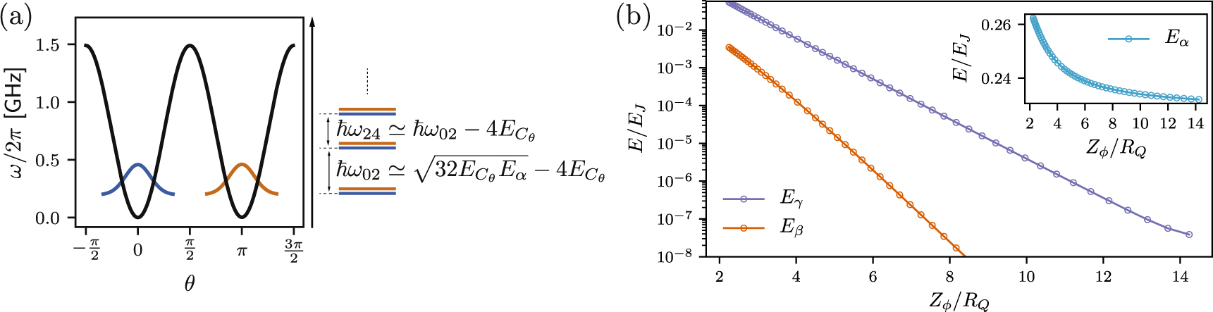