

Abstract
In this study, a 4 bit, 10 giga-samples-per-second analog-to-digital converter (ADC) printed circuit board assembly (PCBA) was designed, manufactured, and characterized for digitizing radio telescopes. For this purpose, an Adsantec ANST7120A-KMA flash ADC chip was used. Together with the field-programmable gate array platform, developed by the Collaboration for Astronomy Signal Processing and Electronics Research community, the PCBA enables data acquisition with a wide bandwidth and simplifies the intermediate frequency section. In the current version, the PCBA and the chip exhibit an analog bandwidth of 10 GHz (3 dB loss) and 20 GHz, respectively, which facilitates second, third, and even fourth Nyquist sampling. The following average performance parameters were obtained from the first and second Nyquist zones of the three boards: a spurious-free dynamic range of 31.35/30.45 dB, a signal-to-noise and distortion ratio of 22.95/21.83 dB, and an effective number of bits of 3.65/3.43, respectively.
1. Introduction
In radio astronomy observations, analog signals are digitized after collecting the incoming waves and are preprocessed using one or more radio antennas. Signal detection is subsequently performed in an auto- or cross-correlation single dish or using antenna array observations for further processing. To increase detection sensitivity and to analyze a wide bandwidth, broadband analog-to-digital converters (ADCs), clocked as high as possible, are necessary.
Given the ongoing advances in technology, electronic devices and components, such as high-speed ADC chips, are expected to process larger amounts of data at higher speeds. Because of demands from radio astronomers for wider bandwidths, designing a faster ADC board at a reasonable cost is essential. Digital signal processing (DSP) is a crucial technology in modern radio astronomy. Design of digital instrumentation requires highly specialized expertise and is a labor, time, and cost intensive process. The past decade has seen a trend toward promoting shared hardware development for components such as interchangeable digitizers, flexible digital hardware processors, reusable DSP libraries, scalable instrument architectures, and flexible monitors, controls, and interfaces. Such developments benefit the radio astronomy community, in particular institutes that can support only a small group of digital developers. The Collaboration for Astronomy Signal Processing and Electronics Research (CASPER), a consortium of several astronomical and engineering institutions worldwide, is one of the major promoters of shared hardware development. The 5 giga-samples-per-second (GSPS) high-speed ADC board (Jiang et al. 2014) and the 10 GSPS ADC board (Figure 1) are our contributions to this consortium and can be used in conjunction with other hardware in the CASPER suite.

Figure 1. 4 bit, 10 GSPS ADC PCBA. The SMA connectors on the left-hand side (from the top) are for a 625 MHz internal clock (CN6), a 10 GHz external clock (CN5), signal input −(CN4), signal input +(CN2) and synchronization signal (CN1), respectively. The jumpers (from the left) are for enabling the digital-to-analog converter (ondac CN7) and the chip-enable control (ceoff CN8). CN9, CN10 and CN11 are for pin cosel1, cosel2 and pin cosel3, respectively; these three jumpers are for the selection of the output clock. Jumper CN12 (pin clk_o_ph) and jumper CN13 (pin c4o_ph) are for the selection of the clock phase in the demultiplexer, ASNT2032. Jumper CN14 (pin cosel1 of ASNT2032) divides the clock output by four in the demultiplexer if it is set too high.
Download figure:
Standard image High-resolution imageThere remain, however, persistent demands from the community for faster ADCs to process wider bandwidths in, for instance, spectroscopic observation, in order to cover widespread spectra lines, or for continuum detection for better sensitivity while reducing the cost and effort in signal processing using ADCs of narrower bandwidths. With regard to our own applications, the ongoing Greenland Telescope (GLT) observation is planning for at least 8 GHz of observation bandwidth; a cosmological experiment for searching highly redshifted molecular lines demands as many GHz of continuum bandwidth as possible. The Submillimeter Array is planning to expand its observational bandwidth up to 16 GHz. These projects would benefit from the successful development of an even faster sampler with a sampling speed of the order of 10 s of GSPS for the CASPER platform. Motivated by these demands, we have developed a 4 bit, 10 GSPS ADC. This paper describes the design, manufacture, and characterization of a 4 bit, 10 GSPS ADC PCBA. The developed PCBA is also targeted toward the CASPER platform, although, in principle, it provides wideband capturing capability for any DSP systems with similar input specifications
The GLT, a radio telescope 12 m in diameter, will be deployed at the Summit Station in Greenland to enable direct confirmation of a super-massive black hole through the observation of its shadow image in the active galaxy M87 (Inoue et al. 2014). The GLT project is led by the Academia Sinica Institute of Astronomy and Astrophysics. The telescope components will be shipped to Thule Air Base, located on the north-west coast of Greenland, in 2016, which will be followed by assembly and first light in 2017. In 2019, the GLT will be established at the Summit Station.
Apart from its very long baseline interferometry applications for 1–2 months annually, the GLT is expected to make single-dish observations (Hirashita 2015) in the 86 GHz–1.5 THz range. For these observations, a mega-channel spectrometer will be designed and manufactured by the present authors. The intermediate frequency (IF) will initially be 4–12 GHz and will subsequently be expanded to 4–20 GHz. We will use the 10 GSPS ADC PCBA together with the ROACH-2 (Parsons et al. 2006, 2008), or the next-generation field-programmable gate array (FPGA) platform of CASPER and its associated gateware library. The open-source library includes functions such as a poly-phase filter bank, fast Fourier transform (FFT), vector accumulation, and auto-correlation, all of which can be linked to form a spectrometer. The commonly used functional blocks are parameterized to allow custom tailoring for various applications.
1.1. Benefits of Faster Sampling Rates and Large Input Signal Bandwidths
Interferometers that can capture and correlate large frequency bandwidths provide the advantages of increased continuum sensitivity and the inclusion of more spectral lines within the observing band.
We have previously discussed the benefits of the digitization of large signal bandwidths (Jiang et al. 2014), and the benefits of the IF system in terms of cost and complexity are approximately 2.4 times the ratio of the ADC sampling rate. The 5 GSPS ADC is operable only in the first Nyquist zone because of limitations in the input signal bandwidth.
The input signal bandwidth of the 10 GSPS ADC is up to 20 GHz, which enables second, third, and even fourth Nyquist sampling. Nevertheless, the IF system can be further simplified.
Figure 2 illustrates the down converter architectures and frequency plan for four 5 GSPS ADCs versus two 10 GSPS ADCs. Both approaches are targeted at capturing an analog input bandwidth of 8 GHz for the GLT system. In the four ADC approach, four filters, four mixers, and four local oscillators are used for frequency separation and down conversion. In the two 10 GSPS ADC approach, only one mixer and two filters are used and consequently the IF system is drastically simplified.

Figure 2. Down converter design comparisons for ADCs operating in different Nyquist zones in the GLT. The upper (a) and lower (b) diagrams represent the down converter architectures for one and two Nyquist zones, respectively. The 5 GSPS ADCs were operated at 4.0 GSPS. PD denotes power divider; LPF denotes low-pass filter.
Download figure:
Standard image High-resolution imageIn the next section, we will describe the design concept and the practicality of selecting the hardware for this work in further detail; the commercial availability of high-speed, wideband ADCs are rather limited. In addition, affordability is another important factor to consider. The technical characterizations of the new PCBA can be found in Section 3, which will be followed by a summary of our work in Section 4.
2. Device Selection and Hardware Design
After developing the 5 GSPS ADC board, the authors searched for faster commercial ADC devices.
Micram developed a 30 GSPS ADC chip in 2010, and Fujitsu released the demonstration version of a 56 GSPS, 8 bit ADC chip in 2011. Both chips have been commercialized (Ellermeyer et al. 2010). Commercial boards from Acqiris (Petriska et al. 2009) were also considered, but the quoted prices of those boards with academic discount to the material cost of this 10G ADC PCBA was about a ratio of 10:1 at least.
Several commercial ADC boards and their associated FPGA platforms—such as Tektronix's TADC-1000, an 8 bit, 12 GSPS ADC—are currently available (Chang & Rowe 2012). Acquitek markets a 10 bit, 10 GSPS ADC board that interleaves two 5 GSPS ADC chips. These commercial boards interleave several identical ADC chips to increase the sampling rate and widen the bandwidth.
After comparing the feasibility and unit price of various chips, we selected the Adsantec Corporation's 10 GSPS, 4 bit flash ADC chip as our key component for the ADC board. This chip doubled the sampling rate and enabled second, third, and fourth Nyquist sampling. During our study, Hittite released a 26 GSPS, 3 bit ADC chip (in August 2012). Several radio astronomical groups are evaluating and testing this chip.
Flash ADCs (Van De Plassche 1994; Razavi 1995), also known as parallel ADCs, provide the fastest conversion of signals from analog to digital. Flash ADCs are suitable for applications requiring extremely high bandwidths. However, because of their high power consumption and relatively low resolution, these converters are limited to high-frequency applications that cannot be addressed by any other means, for example satellite communication, radar processing, and radio astronomy.
The board designed in this study comprises three main components. An ANST7120A-KMA flash ADC chip (Adsantec Corporation) was used as the core component (Figure 1). Forty parallel differential pairs of Z-DOK connectors were incorporated on the right-hand side of the board. The Z-DOK connectors served as the interface for the FPGA platform. The 10 GSPS ADC chip was located on the left-hand side of the board. After passing through the ADC chip, the signals were demultiplexed using two demultiplexing chips. Four sub-miniature version A (SMA) connectors were placed on the left-hand side of the board. One synchronization input, one signal input for digitization, and two clock inputs—10 GHz and 625 MHz for the external and internal phase-locked loop (PLL) reference, respectively—were applied. A simple capacitor served as a high-pass filter. A block diagram of the board is given in Figure 3. The other two chips were digital demultiplexers (Adsantec Corporation).

Figure 3. Block diagram of the 10 GSPS ADC configuration. The ADC chip demultiplexes the output by 1:4 and converts the 4 bit signal into 16 differential pin pairs. Thus, the output data rate is 2.5 GSPS. The additional demultiplexing chips on the board have a 1:2 demultiplexing factor. Consequently, 32 output pin pairs are driven into the Z-DOK connector at 1.25 GSPS according to the low-voltage differential signaling (LVDS) and Z-DOK specifications. The LVDS serves as the interface buffer between the ADC chip and FPGA.
Download figure:
Standard image High-resolution imageThe ADC chip demultiplexes data fourfold. Thus, when the data rate exceeds 2.5 GHz, the low-voltage differential signaling specification is breached. Therefore, an ANST2032-MBL demultiplexer was employed to reduce the data rate to 1.25 GHz, thereby doubling the number of data bits from 16 to 32.
To synchronize two buses using the two demultiplexers, an NB6L11M (ON semiconductor) high-speed analog clock buffer was used. This device buffered the clock rate at 10 GHz, with a clock period of 100 ps. A manually tuned semi-rigid UT-047 cable was introduced in the path of the high-speed clock for aligning the clocks in the two demultiplexers. This adjustable cable provided alignment flexibility and satisfactory data acquisition.
After digitization, the digitized data was buffered by the LVDS interface chips before being output to a high-speed board-to-board Z-DOK connector. The Z-DOK connector transferred the digital data from the board to the FPGA platform.
The board (12.5 cm × 8.5 cm) was a four-layer PCB with Rogers 3003 substrates as the outer layer, which yielded a superior radio frequency range. Conventional FR-4 substrates were placed between the outer layers. The board was comprised of eight trace layers. Its maximum power consumption was approximately 7.2 W. The chip had a 20 GHz analog input bandwidth and digital-to-analog converter (DAC) for verifying the data output.
Realizing the 20 GHz bandwidth was extremely challenging. Baluns were not employed for single-ended-to-differential transformations because differential baluns reduce performance in high-frequency regions. This allowed either differential- or single-ended signals to be applied to the ADC with low-signal attenuation.
A pair of co-planar waveguide traces was used, as shown in Figure 4. The two traces were symmetric and, via holes, were created on the ground plane on both sides of the traces to mitigate electromagnetic interference. Figure 5 illustrates the measured and simulated S-parameter performance of the input traces.

Figure 4. Signal input trace. The upper half shows the layout and the lower half shows the simulation model.
Download figure:
Standard image High-resolution image
Figure 5. Simulation and measurement of two S-parameters of the input signal paths, S11 and S21. The simulation parameters are denoted by the dotted blue (S21) and red (S11) curves. Measurements using high-frequency SMA connectors are denoted by the red (S21) and black (S11) curves. Measurements using regular SMA connectors are denoted by the orange (S21) and blue (S11) curves.
Download figure:
Standard image High-resolution imageANSYS HFSS high-frequency electromagnetic field simulation software was used for the simulation. The test setup for S-parameters was as follows: one pigtail UT-047 wire with an SMA connector was soldered to one of the positive signal input pins of the ADC chip. The SMA connector to the signal input pin was connected to one port of an Agilent PNA-X N5245A network analyzer. The SMA connector at the edge of the board, CN2 in Figure 1, was connected to the other port of the network analyzer.
The PCB was designed for the regular SMA end connector: we used Cinch 142-0701-871. The orange and blue curves in Figure 5 represent the two S-parameters, S11 and S22. The results show that the board is suitable for first to third Nyquist sampling when the regular SMA connector is used. In the orange curve, a −17 dB dip can be observed in the 16 GHz region, which is outside the operating range of the regular SMA connector. The red and black curves show the measured S-parameters with the high-frequency SMA end launch connector; we used Cinch 142-0761-851. The lowest value in the red curve in the entire 18 GHz band is −4.4 dB. The current PCB is not designed specifically for a high-frequency SMA connector, hence the results are poorer than expected. The operation range of this board can be increased to 20 GHz if a high-frequency SMA connector is used with further modifications in the PCB. For the measurements page (Section 3), we used the regular SMA connector.
A block diagram of the chip is shown in Figure 6 (Adsantec 2015). The chip includes a linear input buffer with a tree-type architecture and a current mode logic type input interface with internal 50 Ω single-ended terminations to Vcc. The buffer delivers 15 matching copies of the input analog data signal dp/dn to the 4 bit flash ADC. The ADC creates 15 samples of the input data in thermometer code, which are converted by a thermometer-to-binary encoder into 4 bit binary words at a data rate of f. The ADC thresholds are controlled by signals vrefcrl and vlsbcrl. The encoded data are demultiplexed into 16 bit-wide words at a data rate of f/4 and are sent to the output through 16 low-power LVDS buffers as signals q00p/q00n–q15p/q15n. An optional DAC with an output signal odp/odn, which can be enabled using the control signal ondac, can be used to control the ADC operation.

Figure 6. Block diagram of the ADC chip.
Download figure:
Standard image High-resolution imageAll operations are synchronized by the internal clock multiplication unit based on the PLL with an integrated divider and an external loop filter connected to pin ftr. The block can operate in two different modes controlled by the signal ceoff: clock multiplication (when the PLL is on, a reference clock is applied to pins crp/crn) and clock division (when the PLL is off, an external high-speed clock is applied to pins cep/cen).
In both modes, the divider generates internal clock signals in divisions of 2, 4, 8, and 16. These signals are sent to different internal blocks. In the CMU's second operation mode, the divider can be preset by external signal, res, to allow synchronization of parallel-connected ADCs. A PLL lock control output is also provided.
The primary interface for digital inputs, outputs, and power for this ADC board is a Z-DOK connector (Tyco 2003; see Figure 1). This connector provides 40 pairs of controlled impedance transmission lines (100 Ω line-to-line), and each pair consists of signal+, signal-, and ground. Two ANST2032-MBL demultiplexer outputs, which have 32 pairs of LVDS, are routed directly to the Z-DOK without re-clocking or buffering. The remaining 8 pairs of the connector are used for clock, synch, telemetry, and control signals. For DC power (+5, +3.3, +2.5, and +1.8 VDC), Z-DOK provides 24 additional non-impedance-controlled utility connections. For the Z-DOK connector, the single-channel input mode provides a maximum data rate of 1.25 GBPS, which is well within the maximum specified rate of 6.2 GBPS.
3. Calibration and Performance
The test setup used for calibration and characterization is illustrated in Figure 7. The input to the ADC under test was stimulated as a variable frequency continuous wave (CW) tone at −8.5 dBm. At this power level, the time domain sine wave occupied half the full range of this ADC device (Vpp = 0.2377 V).

Figure 7. Calibration and test setup for the ADC. A CW source from a Hewlett Packard (HP) signal generator, 83630B, is used to stimulate the ADC under test. ROACH-2 and a Linux PC are used to capture and process the digitized data from the ADC. The internal 10 GHz clock is phase locked to a Valon frequency synthesizer board at 625 MHz. A 10 MHz clock signal generated by the HP signal generator was fed to the Valon board as the phase-lock reference to the output frequency.
Download figure:
Standard image High-resolution imageTwo adjustable voltages are available for the input signal reference and least significant bit reference, namely vrefcrl and vlsbcrl, respectively. Those are translated as gain and offset for the ADC control, respectively. For optimizing the data capture, we created an automatic tuning program to tune those two parameters through a serial peripheral interface bus. It first adjusts the offset to achieve zero DC offsets. Then, the program gradually tunes the gains and compares the read-back amplitudes. Subsequently, the program terminates the adjustments and saves the gain and offset parameters in a nonvolatile memory position 1024 in the digital potentiometer AD5235.
We placed a 3 dB attenuator at the input of the board for characterizing the spur-free dynamic range (SFDR), signal-to-noise and distortion (SINAD), and effective number of bits (ENOB). We tuned the input power of the board to −8.5, −5.5, −4.5, and +9.5 dBm for the first, second, third, and fourth Nyquist zones, respectively.
Furthermore, we performed a FFT on 4096 spectral channels for 8192 samples. We calculated and carefully tuned the CW signals such that they were concentrated on the center of the spectral bin, which helps avoid leakage to the adjacent bins. We chose eight discrete CWs per Nyquist zone, spaced at an interval of approximately 500 channels, for the characterization.
The SFDR is given by Equation (1) (Section 8.8.2, of IEEE 2010):

where Ainput is the amplitude of the input tone, and the nominator is the maximum of either the harmonic or spurious signals appearing in the acquired spectrum.
The SFDR for the ADC board was characterized by inputting a single-frequency tone into the ADC and measuring the ratio of the desired tone to the maximum undesired spur at the FFT output (IEEE 2010). The results are plotted in Figure 8. The SFDR specification for the Adsantec device at the first and second Nyquist zone is 30.13/28.78 dB, respectively, which is typical for a 3.9/7.8 GHz input signal. Our measured results at approximately the same frequency are 32.27/29.49 on average.

Figure 8. SINAD and SFDR of three boards characterized from the first Nyquist zone to the fourth Nyquist zone.
Download figure:
Standard image High-resolution imageSINAD is defined as the ratio of the root mean square (rms) of signal amplitude to the root sum square of the noise and all other spectral components, including spurs and harmonics (IEEE 2010).
To determine the SINAD, the NAD must be calculated first, for which we fit a sine wave to the record at the chosen frequency. Next, we computed the estimate of the rms value of the noise and distortion, as shown in Equation (2):

where is the sample data set, is the data set of the best-fit sine wave, and M is the number of samples in the record.


The SINAD is given by Equation (3):

where
The results are plotted in Figure 8. The SINAD specification for the Adsantec device at the first and second Nyquist zones is 22.15/21.19 dB, respectively, typical for a 3.9/7.8 GHz input signal. Our results obtained at approximately the same frequency, 3.6/8.0 GHz, are 23.0/20.34 on average. The performance of board No. 8 (light blue curve) is worse than board No. 6 (black curve) and board No. 7 (red curve). This is due to the ADC chip being replaced by hand, meaning it performed worse.
SINAD is related to ENOB. ENOB is defined by IEEE (Section 9.4 of the IEEE 2010) as follows: for an input sine wave of specified frequency and amplitude, after correction for gain and offset, the effective number of bits (ENOB) is the number of bits of an ideal ADC for which the rms and distortion of the ADC are under test. ENOB is given by
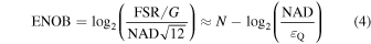
where N is the specified number of bits in the ADC, FSR is the specified full-scale range of the ADC, G is the measured gain (nominally = 1), NAD is the rms noise and distortion, and εQ is the rms ideal quantization error.
The ENOB specification for the Adsantec device in the first and second Nyquist zones is 3.39/3.23 bits, respectively, which is typical for a 3.9/7.8 GHz input signal. Our results are shown in Figure 9. Our results at approximately the same frequencies, 3.6/8.0 GHz, are 3.74/3.14 on average, as shown in Figure 9.

Figure 9. ENOB of three boards characterized from first Nyquist zone to fourth Nyquist zone.
Download figure:
Standard image High-resolution image3.1. Optimal Input Noise Power
This ADC board can be used for astronomical applications where the input signal consists largely of Gaussian noise. A question arises here: what is the optimum input-signal drive level relative to Vfull-scale of the ADC device? Underdriving the ADC results in a lower SINAD and ENOB, whereas overdriving leads to clipping and generation of undesired harmonics.
The IEEE method for determining the optimal input drive is by performing a noise-power ratio (NPR) test. This test consists of a broadband noise source with a notch filter to remove a portion of the noise prior to inputting it to the ADC under test. Our test setup for the NPR test is illustrated in Figure 10. First, a 16 GHz wideband noise source, NW10M16G-M by Noise Wave, was used to inject a noise signal into a 4 GHz low-pass filter and then into a tunable notch filter, 3TNF-1500/3000-N/N by K&L Microwave, with a tuning range of 1.5 GHz to 3.0 GHz. An adjustable attenuator, 8494B by Keysight, was used to attenuate the input power to determine the optimal value of the NPR. An FFT was performed on the digitized ADC output and the NPR (Equation (5)). The ratio of the desired noise to the undesired residual noise in the notched portion of the spectrum was characterized at different input power levels.

where PNo and PNi are the outside and inside notch power spectral densities (Section 8.10 of IEEE 2010).

Figure 10. NPR test setup.
Download figure:
Standard image High-resolution imageThe optimum drive occurs when the NPR is at the maximum. For an ideal 4 bit ADC, the maximum NPR is 19.4 dB and occurs at a loading factor of −8.6 dB, which is equivalent to an input drive of −9.1 dBm at the input point of the board. The loading factor is the signal input level to the full-scale input range in decibels. For this, the maximum NPR of three boards at 1.5, 2.0, and 2.5 GHz should be between 15.8 and 17.6 dB, as depicted in Figure 11. It occurs at a loading factor of approximately −7.6 dB, which is equivalent to an input drive of −8.1 dBm at the input of this board. Figure 12 shows the spectra of the NPR tests at three different frequencies. The roll-off at frequencies less than 1 GHz and more than 3 GHz is due to the notch filter response.

Figure 11. NPR performance. The red trace represents the NPR for an ideal 4 bit ADC. Black, brown, and blue traces represent three different boards. Short-dashed, long-dashed, and solid lines represent the NPR at 1.5, 2.0, and 2.5 GHz, respectively.
Download figure:
Standard image High-resolution image
Figure 12. Overlapped spectra with notch filter at 1.5 GHz (blue curve), 2.0 GHz (black curve), and 2.5 GHz (red curve). 100 spectra were averaged for each of the notch traces.
Download figure:
Standard image High-resolution image
4. Summary
In this study, we developed an ADC board that permits digitization of up to 5 GHz of analog-signal bandwidth with 4 bit quantization. Previously, we developed a 5 GSPS ADC for the CASPER community. The current effort was geared toward applications such as the GLT (Hirashita 2015), AMiBA (Ho et al. 2009) and the Smithsonian Submillimeter Array (SMA), where the receiver output bandwidths are 16, 16, and 18 GHz, respectively. The developed device can capture larger portions of the IF spectrum, which reduces the complexity and cost of the IF distribution system.
The SFDR, SINAD, and ENOB of the ADC board were characterized over its operating bandwidth. The ADC board is functional for first and second Nyquist sampling as well as for third Nyquist sampling if an equalizer is employed to flatten the band. For the first and second Nyquist zones (i.e., 0–10 GHz), the average SFDR, SINAD, and ENOB are 31.35/30.45 dB, 22.95/21.83 dB, and 3.65/3.43 bits, respectively, all of which refer to an input drive level of −6 dB fs. We recommend using a high-frequency SMA connector and a modified PCB if third and fourth Nyquist sampling is necessary. Finally, for Gaussian-noise-dominated applications, we recommend an input drive level of −8.1 dBm (−7.6 dB loading factor).
The authors wish to acknowledge the assistance and support of the CASPER community, especially the University of California at Berkeley, and the MeerKAT in South Africa. This work was funded by Academia Sinica.