

Abstract
Objective. Current neural probes have a limited device lifetime of a few years. Their common failure mode is the degradation of insulating films and/or the delamination of the conductor–insulator interfaces. We sought to develop a technology that does not suffer from such limitations and would be suitable for chronic applications with very long device lifetimes. Approach. We developed a fabrication method that integrates polycrystalline conductive silicon carbide with insulating silicon carbide. The technology employs amorphous silicon carbide as the insulator and conductive silicon carbide at the recording sites, resulting in a seamless transition between doped and amorphous regions of the same material, eliminating heterogeneous interfaces prone to delamination. Silicon carbide has outstanding chemical stability, is biocompatible, is an excellent molecular barrier and is compatible with standard microfabrication processes. Main results. We have fabricated silicon carbide electrode arrays using our novel fabrication method. We conducted in vivo experiments in which electrocorticography recordings from the primary visual cortex of a rat were obtained and were of similar quality to those of polymer based electrocorticography arrays. The silicon carbide electrode arrays were also used as a cuff electrode wrapped around the sciatic nerve of a rat to record the nerve response to electrical stimulation. Finally, we demonstrated the outstanding long term stability of our insulating silicon carbide films through accelerated aging tests. Significance. Clinical translation in neural engineering has been slowed in part due to the poor long term performance of current probes. Silicon carbide devices are a promising technology that may accelerate this transition by enabling truly chronic applications.
Export citation and abstract BibTeX RIS
1. Introduction
The last decade has seen a wealth of new technologies for electrophysiological recording and stimulation. While these devices have addressed unmet needs in acute and short-term use, translation from lab to clinic has been slowed, in part, due to the poor performance of neural implants in the true long term (>5 yr implant lifetime). Brain machine interface (BMI) translation, for example, has been hampered by this issue: accurate decoding of neural activity rapidly decays with the degradation of the recorded signals, which is a consequence of the deterioration of recording electrodes in neural implants. These effects have been extensively studied in Utah arrays, the mainstay of current clinical cortical interfacing although the same degradation is observed in all other commercially available probes. Barrese et al [1] have made a comprehensive study of the failure mode of 62 of these arrays implanted in non-human primates over a span of about a decade. After one year over 70% of the arrays failed due to a combination of biological, material and mechanical factors; just two arrays remained active after four years and one array made it to 6 yr (even this is an optimistic picture since an array of 100 electrodes was still considered active if just 1 out of 100 channels was able to record single units). Other kinds of neural probes also show significant material degradation [2]; tungsten microwires lasted nine months on average [3] and six months in the case of silicon planar arrays [4]. We posit that the longevity of neural probes is ultimately determined primarily by material factors. Specifically, once the implant has survived the attacks of the body's acute immune response and glial scarring has ceased, if the foreign object is accepted by the body, continued operation requires the electrode insulation to remain stable: there must be no delamination of the insulator due to water penetration nor failure of the insulator-conductor material interface at electrodes sites (or along the conductor).
Silicon carbide (SiC) has all the characteristics necessary to make highly reliable neural implants. SiC is chemically inert, which means it will not corrode in bodily fluids [5]. There is a large body of literature exploring the use of SiC for sensors designed for high temperature, highly corrosive environments [6]. Additionally, SiC has been shown to be more biocompatible than silicon in vitro and in vivo [7–9], is a wide bandgap semiconductor (making it feasible to produce insulating or conducting variants of the material), is compatible with silicon microfabrication techniques and is very flexible when deposited in thin films [10]. The superiority of SiC has been known to the neural engineering community for several years [7, 11]; some groups have demonstrated the effectiveness of silicon carbide as protective coating in retinal implants [5] and others have worked to integrate conductive and insulating silicon carbide in test structures [12].
In this work, we report a fabrication process and an implantable device that uses polycrystalline conductive silicon carbide at the recording site and amorphous silicon carbide as the only insulation. An internal metal interconnect is completely embedded and supported by the SiC films and is used to reduce the resistance of long traces. The result is an electrode array that, to the physiological fluid, appears simply as a single SiC sheet wherein external boundaries between conducting and insulating layers are seamless. We believe this approach has the potential to disrupt the way chronic thin film interfaces are currently produced and provide a clear pathway to decades-long implantable electrophysiology.
2. Materials and methods
2.1. Fabrication process
The fabrication process flow is shown in figure 1. Devices are fabricated on 6" p-type test grade silicon wafers. Wafers are cleaned in a piranha bath at 120 °C for 10 min, followed by a rinse in 18 M water, immersion in 1:10 HF at room temperature for 1 min, a rinse in 18 M
 water and spin drying. A layer of thermal oxide 1 μm thick may be grown by wet oxidation (Tylan furnace, 1050 °C, atmospheric pressure, 3 h) immediately followed by deposition of 700 nm of polycrystalline n-doped silicon carbide by low-pressure chemical vapor deposition [13] (LPCVD, Tylan furnace, 800 °C, 170 mTorr, 30 sccm methylsilane, 15 sccm dichlorosilane, 2 sccm ammonia, 48 sccm H2, 2.5 h) and then followed by deposition of 500 nm of silicon dioxide by plasma-enhanced chemical vapor deposition (PECVD, Oxford plasma lab100, 1000 mTorr, 1000 sccm N2, 750 sccm N2O, 5 sccm 10%SiH4/Ar, 20 W, 38 min). Recording sites and bondpads are defined by standard photolithography using g-line photoresist (OCG 825 35cs, Fujifilm, Valhalla, NY), with a UV hard bake step to improve selectivity in the plasma etch. Next, the oxide layer is patterned using reaction ion etching (RIE, Lam Research, 70 mTorr, 150 sccm Ar, 10 sccm CHF3, 40 sccm CF4, 705 W RF power, 150 s) followed by patterning of the n-SiC by RIE (Lam Research, 12 mTorr, 125 sccm Cl2, 75 sccm HBr, 100 sccm CF4, 300 W RF power, 150 W RF bias) and photoresist strip in oxygen plasma. A contact profilometer is used to measure the height of the n-SiC/SiO2 stack in order to estimate the degree of overetch in the bottom oxide layer and determine the necessary thickness of the upcoming insulating film.
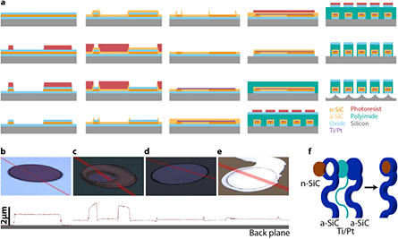
Figure 1. (a) Schematic of fabrication process. Confocal image and surface profile of: (b) SiO2 on n-SiC pillar recording site on a thermal oxide backplane. (c) Opening through a-SiC on top of recording site exposing n-SiC. Profile shows that height of n-SiC pillar closely matches height of a-SiC backplane. (d) n-SiC rec site embedded in a-SiC backplane after freestanding a-SiC pieces were removed in ultrasound bath. (e) Metal interconnect on top of n-SiC recording site. (f) 3D model of SiC electrode at recording site showing metal interconnect completely embedded in n-SiC and a-SiC.
Download figure:
Standard image High-resolution imageJust prior to the deposition of the first insulating layer, wafers are cleaned in a piranha bath at  C for 10 min followed by a rinse in 18 M
 water and spin drying. A layer of a-SiC is deposited conformally by PECVD (Oxford plasmalab100, 300 mTorr, 500 sccm Ar, 30 sccm CH4, 7.5 sccm 10%SiH4/Ar, 25 W–80 W, 1 h 8 min); argon ion sputtering is used to remove any native oxide that may be present on the n-SiC walls. Chuck temperature is held at 350 °C. The thickness of the a-SiC layer varies with the height of the n-SiC recording site and the amount of overetch during patterning of the recording sites; the a-SiC layer is typically between 550 and 1000 nm. To open electrical access to the recording sites, a mask of g-line photoresist and standard photolithography are used with a UV hard bake step of the resist to improve selectivity during plasma etch. The portion of insulating silicon carbide on top of the doped silicon carbide features is plasma etched until the silicon dioxide separating the two types of carbide is exposed (technics-c, 13 sccm SF6, 21sccm He, 200 mTorr, 150 W). After stripping the photoresist in O2 plasma, the oxide in-between the two types of carbide is etched in a 1:10 HF bath at room temperature. Next, the free standing portions of a-SiC left after the oxide has been etched are removed in a 10min ultrasonic water bath. Then, a patterned metal stack of 150 nm Pt on 5 nm Ti is obtained by standard lift-off process and deposited by electron beam evaporation.
Next, a second layer of insulating a-SiC is deposited by PECVD with the exact same parameters as the first a-SiC layer described above. CF4 etch followed by argon sputter etch is used to etch any oxide that may have formed on the first a-SiC layer; the vacuum seal is not broken. To pattern this layer, 2 um of g-line photoresist is spun and patterned with standard photolithography techniques and then plasma etched in the same manner as the first a-SiC layer. This time, the a-SiC and the thermal oxide are plasma etched down to the silicon substrate with the SF6 chemistry described before. At this stage, the electrode fabrication is finished and what follows is the addition of a backing layer and release procedures. We use a backing layer of 4 μm of polyimide PI-2611 (HD microsystems, Wilmington, DE) which is spin coated and cured as recommended by the manufacturer. The outline of the devices and access holes are patterned on the polyimide by oxygen plasma using a hard mask of silicon dioxide deposited by PECVD and g-line photoresist. Devices are released by XeF2 etching of the silicon that is in direct contact with the thermal oxide; the gas is able to reach the silicon through access holes opened in the backing layer. Once electrodes are released, an HF dip is used to remove the thermal oxide if necessary. Alternative backing layer material can be used provided it is resistant to XeF2 and HF.
2.2. Assembly and characterization
Thin film SiC ECoGs and polyimide ECoGs (used as controls, refer to the supplemental information available at stacks.iop.org/JNE/14/056006/mmedia) were assembled on printed circuit boards (PCB) using anisotropic conductive film (ACF) as previously described [14, 15]. Briefly, ACF 7379 tape (3M science applied to life) was prebonded to the ACF bondpad area of the PCBs using an Ohashi HMB-10 table-top bonder equipped (5 s, 90 kg cm−2, 90 °C at bond site, blade set to 135 °C), then the bondpads of the ECoGs were aligned to the footprint on the PCB under a microscope and tacked to the tape with a soldering iron. Finally, permanent bonding was done using Ohashi Bonder equipment (30 s, 160 kg cm−2, 160 °C at bond site, blade set to 235 °C).
Electrolyte interface spectroscopy (EIS) was done with a NanoZ (Tucker Davis Technology, Alachua, Fl) by immersing the recording sites of the ECoGs and the reference wire in  . Recording sites were electroplated with platinum black (YSI 3140 platinizing solution, Fondriest Environmental, Fairborn, OH) using the NanoZ for 10 s at −2 μA. EIS was performed before and after electroplating.
2.3. In vivo recordings
All animal experiments were performed in accordance with the University of California-Berkeley Animal Care and Use Committee regulations. Neural recordings from the central nervous system (CNS) and the peripheral nervous system (PNS) were done in adult male Long-Evans rats.
2.3.1. Primary visual cortex.
An adult male Long-Evans rat was anesthetized with urethane and placed in a stereotaxic instrument. ECoGs were acutely implanted in the right primary visual cortex, and visual stimuli was presented contralaterally to the left visual field on an LCD monitor. Stimuli consisted of drifting sinusoidal gratings at 100% contrast ratio. The direction of motion of each stimulus was randomly chosen between 45 and 360 degrees in 45 degree intervals. Stimuli were presented in a series of trials consisting of a 2 s zero contrast display, followed by 2 s of a drifting grating at the randomly chosen orientation, followed again by a 2 s zero contrast display. Trials were repeated at 15 s intervals. Control trials consisted of a zero contrast display during the stimulation period of the trial, resulting in the presentation of a zero contrast display during the entire 6 s period.
Signals from the surface of the rat primary visual cortex were sampled at 25 kHz using a TDT RZ2 digital signal processor and PZ2 pre-amplifier (Alchua, FL). Data were analyzed using custom routines written in Python. Spectral estimation of field potential activity was done using the multi-taper method [16]. A total of 5 tapers were used with a time-bandwidth product of 3. To calculate spectrograms displaying spectral power over a given trial interval, spectral estimates were computed every 50 ms with a window size of 750 ms. Each individual frequency band of the resulting spectrogram was normalized to its own mean power over the entire time interval.
2.3.2. Sciatic nerve stimulation.
SiC electrode arrays were used to record from the peripheral nervous system. The active site of a SiC electrode array was wrapped around the right sciatic nerve of an anesthetized adult Long Evans rat in an acute experiment as shown in figure 5(a). Electrical stimulation was delivered through stainless steel needles to the biceps femoris muscle ipsilateral to the electrode array. The stimulation consisted of square pulses of 10 μs at 0.5 Hz that varied in amplitude between 0.5 and 1.2 mA. Electrical stimulation of the contralateral muscle was performed as a control.
Data were collected on 32 channels using TDT RZ2 digital signal processor and PZ2 pre-amplifier at a sampling rate of 25 kHz. Data analysis was done using custom Matlab scripts; data were high pass filtered to remove the DC offset and stimulus triggered averages were calculated for each of the stimulus amplitudes used.
2.4. Longevity test of a-SiC films
2.4.1. a-SiC film deposition parameters.
Several films of a-SiC were deposited on p-type or n-type 6" silicon wafers with different parameters with the objective of evaluating the best performing film in terms of chemical inertness, electrical insulating properties and pinhole density. The parameters tested included precursor flow rates, precursor ratio, diluting gas, diluting gas flow rate and ratio, high frequency generator use, high frequency power, low frequency power and process pressure. A complete list of the recipes described in this manuscript is included in the supplementary information.
2.4.2. Longevity test.
The long term insulating performance of a-SiC films was tested at the wafer level by measuring leakage currents through the film. Several a-SiC films with multiple thicknesses and deposition parameters were deposited on p-type and n-type silicon wafers, then a  piece was cleaved and an inverted PDMS cup was O2 plasma bonded to the a-SiC film (90 s, low power, air plasma, Harrick Plasma, Ithaca, NY). The PDMS cup created a sealed chamber with the carbide film inside wherein PBS solution was contained. Each sample to be tested was placed on an aluminum plate and secured to it with screws in order establish good electrical contact between the silicon carrier and the metal plate; a platinum wire was then pierced through the PDMS so that the wire was completely immersed in the PBS. The longevity test consisted of heating up the system so that the substrate was at temperatures of 90–96 °C; a DC bias of 3.24 V was then applied with the aluminum plate being the cathode and the platinum wire the anode. Currents were measured by placing a 1 M
 resistor in series with the sample and measuring the voltage on the resistor.
In order to test multiple samples simultaneously, a digital multiplexer was used to select the resistor to which the positive terminal of a multimeter was connected. A custom Python script running on a Raspberry Pi was used to select the input of the multiplexer, control the multimeter, measure temperature and log all data.
Once the aging of each film was completed, the PDMS was removed from the sample in order to examine the aged film. Films were first inspected visually by comparing the color of the portion of the film exposed to solution to the portions of the film not exposed to solution (and to the film on the rest of the wafer); micron-thick films deposited on reflective surfaces change color with even minute changes in thickness, a fact long used for qualitative scoring of etching in the semiconductor industry. Film thickness was then measured by ellipsometry and in some cases by scanning electron microscopy (SEM); film thickness of the aged film was compared to the closest portion of the film on the same sample that was not exposed to the solution.
Finally, some samples were subject to 30 min of XeF2 etching in order to determine changes in film composition and to expose possible pinholes created by the aging test; new pinholes in the film allow XeF2 gas to access the silicon, creating large defects easily identifiable by visual inspection under the microscope.
3. Results
3.1. Recording arrays can be fabricated using SiC technology
The bottom panel of figure 1 shows confocal images of recording sites embedded in the amorphous silicon carbide at different fabrication stages. The initial doped SiC pillar (700 nm) with the oxide on top (500 nm) are about 1200 nm above the backplane of the wafer (figure 1(b)); the amorphous SiC matches the height of the n-SiC and due to the conformal deposition of the a-SiC the height of the whole structure is still 1200 nm relative to the a-SiC backplane (figure 1(c)). Once a portion of the a-SiC and the PECVD oxide between the n-SiC and the a-SiC are etched, the surface of the n-SiC pillar is exposed and is leveled with the a-SiC backplane. This becomes clearer once the free standing a-SiC on top of the recording site is removed with ultrasound (figure 1(d)). Finally, the metal easily contacts the doped carbide to connect recording sites and bondpads (figure 1(e)).
During the fabrication process, several critical performance test were carried out. First, the lack of etching of the thermal oxide underneath the carbide features demonstrates that the interface between the doped and the amorphous carbide was properly sealed. As a control, recording sites or bondpads that showed defects at the interface due to photolithography errors provided counter examples of a properly sealed interface and were easily spotted during the HF immersions (see the supplementary information). After depositing and patterning the second layer of insulation, the metal traces were completely embedded within the silicon carbide as shown in figure 2(d).

Figure 2. (a) Assembled SiC electrode arrays. (b) SiC electrode array as released from the wafer before assembly. (c) Active area of SiC electrode arrays for intracortical (top) and surface (bottom) recordings. (d) Zoomed-in optical image of recording sites.
Download figure:
Standard image High-resolution imageTo demonstrate the applicability of the process to other types of neural probes, two types of arrays were fabricated: microECoG arrays (with designs for rodents and non-human primate), and intracortical arrays (which can be inserted by means of a silicon stiffener and water soluble adhesives as demonstrated by Felix et al [17]). Figure 2(a) shows the four variants of these devices fabricated on a single wafer and figure 2(c) is a close up of the active area of the 64 channel ECoG and the 32 channel intracortical array.
The typical yield of the assembly process was >60% working channels; channels failed due to a combination of lack of connection between the thin film features and the PCB during ACF bond or lack of connection between the metal trace and the doped SiC due to a height miss match between the doped SiC recording sites (or bondpads) and the insulating carbide which could not be overcome by the thickness of the metal trace. In vitro characterization showed typical EIS performance with impedance at 1 kHz of ∼30 k after platinum black electroplating. The baseline noise in the 1 Hz–1 kHz band was 15–37μVrms and ∼4μVrms in the high gamma band of 60–200 Hz (figure 3). These values are comparable to those reported for silicon planar arrays of similar dimensions [4, 18] and are slightly higher than the noise floor of our own control polyimide electrode arrays (10 μVrms and 3.7 μVrms for the 1 Hz–1 KHz and 60–200 Hz bands, respectively).

Figure 3. (a) Impedance magnitude and phase of recording sites before electroplating. Gray traces represent each electrode measured and black traces are averages. (b) Impedance magnitude and phase of recording sites after electroplating. Gray traces represent each electrode measured and black traces are averages. (c) Baseline noise measured in saline in the 1 Hz–1 KHz band and high gamma band (60–200 Hz), top and bottom respectively, for three representative channels.
Download figure:
Standard image High-resolution image3.2. Silicon carbide devices are suitable for interfacing with CNS and PNS
3.2.1. Activity can be recorded in the primary visual cortex.
A 64 channel SiC ECoG was used to measure the neural responses of the rat primary visual cortex (V1) to visual stimuli that consisted of sinusoidal gratings moving across a computer screen at various orientations. Figure 4(a) shows the location of the active area of the array in V1. Increases in the gamma-band activity were observed in all of the stimulation trials, and some electrodes recorded apparent orientation-tuned responses. Figure 4(b) shows the neural response recorded in one channel during a period of stimulation of bars in the  orientation; the green line indicates the onset of stimulation and red line the offset. A significant increase signal power in the gamma and high gamma bands was observed with a delay of about 100 ms. An example of orientation tuning is shown in figure 4(c) where the strongest activity was observed in response to the 270° and 225° stimuli orientations and the least strong response for 45° and 180°. In the macro scale, neural responses were distributed along the cortex as shown in figure 4(d). As expected, the control stimuli fail to elicit a neural activity in response to the onset of the stimulation; this is shown in figure 4(e). Activity seen in some of the channels during the control trial is outside the stimulation window.

Figure 4. (a) Photo of SiC ECoG implanted on primary visual cortex of a rat. (b) Spectrogram of neural response to visual stimulus. Green line is stimulus onset and red line is offset. (c) Spectrograms of representative channel with orientation tuning. Center plot is control trial and plots around it corresponds to all orientations tested. (d) Whole ECoG array spectrograms during visual stimulation with bars at 270°. (e) Whole ECoG array spectrograms during control trial.
Download figure:
Standard image High-resolution imageRecordings from a polyimide ECoG control array are included in the supplemental material.
3.2.2. Compound action potential can be recorded in peripheral nerves.
Figure 5 shows the peripheral nerve response to electrical stimulation of the biceps femoris muscle ipsilateral to a SiC array. The active area of the array was wrapped around the proximal sciatic nerve as shown in figure 5(a). Electrical pulses with different amplitudes were applied to elicit the expected sigmoidal recruitment response curve. Figure 5(b) shows the recorded response to each of the amplitudes tested and figure 5(c) shows a summary of the response of the sciatic nerve as the amplitude of the electrical stimulation increases. For low stimulation amplitudes, 0.5 mA and 0.6 mA, the average peak-to-peak amplitude of the combined action potential was the smallest, and this amplitude rapidly increased for amplitudes of 0.7 to 0.9 mA and saturated at around 1 mA. Figure 5(d) shows the nerve response for measured channels during 0.8 mA stimulation. When electrical stimulation was applied to the muscle contralateral to the array, no action potential was observed regardless of the amplitude of the stimulation.
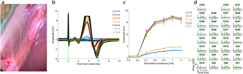
Figure 5. (a) Photo of SiC electrode array implanted on sciatic nerve. (b) Signal recorded on one representative channel showing sciatic nerve response to electrical stimulation. Individual responses have been aligned to the artifact caused by the electrical stimulation. Each color represents an stimulus amplitude and black traces are averages. 0.5 mA was below threshold and failed to elicit an action potential strong enough to be observed. When stimulation was increased to 0.6 mA, a compound action potential of small amplitude was observed 10% of the time. Stimulation at 0.7 mA or higher reliably elicit an action potential every time the muscle was stimulated. (c) Five representative channels showing sciatic nerve saturation as stimulation amplitude increased. The plot shows the average peak to peak amplitude of the recorded action potential as a function of stimulation amplitude. (d) Example of the signals recorded by the whole electrode array for one representative stimulation amplitude. Each plot corresponds to one electrode. Some channels that recorded significantly smaller signals or no signal at all likely correspond to those whose impedance was too high.
Download figure:
Standard image High-resolution image3.3. Silicon carbide insulation remains stable after accelerated aging tests
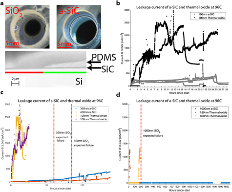
Over 50 different films of PECVD a-SiC on silicon wafers were subjected to room temperature and accelerated aging (96 °C) leakage current tests (see Methods). Films less than 150 nm thick were aged up to 24 h while films thicker than 150 nm were aged for up to 1600 h. Every a-SiC film that was subject to the aging test remained visually intact regardless of the length of the experiment; the color of the exposed film was indistinguishable from the control film. In contrast, thermal oxide control samples were clearly etched and in some cases the silicon carrier was completely exposed. Representative optical photographs of this visual inspection are shown in figure 6(a).
Figure 6. (a) (Top) Example of 24 h aged thermal oxide and a-SiC films. Oxide film has been etched leaving the silicon carrier completely exposed in some regions while a-SiC film looks undamaged. (Bottom) SEM image of a 280 h aged a-SiC film showing that the a-SiC has no observable change in thickness between the section exposed to the PBS and the section covered by the PDMS. The green line indicates the portion of the film under PDMS and the red line indicates the portion exposed to the solution. (b) Leakage currents of 100 nm a-SiC and 100 nm thermal oxide on p-type silicon carrier for accelerated aging test lasting up to 25 h. (c) Leakage currents of >350 nm a-SiC films and oxide films on p-type silicon carrier. (d) Leakage currents of 1000 nm a-SiC, 180 nm SiO2 and 850 nm SiO2 on n-type silicon carrier.
Download figure:
Standard image High-resolution image
Film thickness measurements by ellipsometer of films up to 130 nm thick showed a change in film thickness of less than 5 nm for all films aged up to 110 h and less than 2 nm for films aged for up to 24 h. A 450 nm SiC that was aged for 280 h had no observable etched material as evidenced in the SEM image shown in figure 6(a) (the portion of the film covered by PDMS is of the same thickness as the portion of the film exposed to the solution; film thickness was measured by micro-spectrophotometry to confirm the lack of etched material). Thermal oxide films etched at rates of 70 nm d−1–150 nm d−1.
Leakage current data for thin (100–117 nm) a-SiC films are shown in figure 6(b); the leakage currents were <500 nA cm−2 at ∼96 °C for the entire duration of the experiment while leakage currents for the control samples increased rapidly within 3 h up to about 2.5 μA cm−2. When the temperature was dropped from ∼96 °C to room temperature, leakage currents returned to low levels (50 to 100 nA cm−2 or 2× the original room temperature value before testing began). In contrast, room temperature leakage for controls (100 nm thermal oxide) went from <1 nA cm−2 to 1 μA cm−2. Thicker a-SiC films (360 nm and 450 nm) were aged for several days and performed better than how thermal oxide controls would: leakage currents for the 360 nm film started at about 13 nA cm−2 at 3.24 V and ∼96 °C and remained about this value for up to 24 h at which point the current steadily increased for a couple of hours to a value greater than 30 nA cm−2. After 60 h of aging, leakage currents of this a-SiC film was about 70 nA cm−2 at 96 C while the current at room temperature after over 100 h of aging was as low as 33 nA cm−2. A thermal oxide film 360 nm thick would have been expected to fail at about 60 h of aging. The 450 nm a-SiC film had a similar trend while exhibiting longer lasting insulating properties: leakage currents at high temperature remained below 50 nA cm−2 for up to 90 h, longer than the expected failure time of a 450 nm thermal oxide film. This a-SiC film had leakage currents below 100 nA cm−2 for up to 140 h at which point currents rose rapidly during the following 10 h and then continued to increase at a slower rate for the next several days reaching a maximum of about 500 nA cm−2 at high temperatures. Finally, 1000 nm a-SiC films deposited on n-type silicon carrier remained good insulators maintaining leakage currents of less than 1 nA cm−2 at high temperatures for up to 1600 h while the 1000 nm thermal oxide fails at ∼200 h as shown both by Fang et al [19] and linear interpolations of our own data (observed failure times for 100, 180 and 850 nm thermal oxide films).
XeF2 etching of samples that failed in the aging process during the first few days showed point defects in the a-SiC films. However, the number of point defects on a section of SiC film exposed to PBS was comparable to the number of point defects in the section of the film outside the PDMS chamber, indicating that the accelerated aging likely did not produce more pinholes.
3.4. Silicon carbide is more chemically inert than other silicon-based materials
Etch rates of as-deposited PECVD a-SiC films in XeF2 were highly dependent on the deposition parameters, but in most cases XeF2 selectivity to Si over SiC was excellent, and even selectivity of thermal oxide over SiC was good. Typical etch rates of a-SiC films were 0.5 nm min−1 with an estimated Si:SiC selectivity of at least 2500:1. Some a-SiC had etch rates as low as 1 nm h−1 and for one particular recipe there was no measurable change in film thickness after 2 h of exposure to XeF2. In addition, LPCVD SiC and PVD SiC did not etch in XeF2.
4. Discussion
We introduce a fabrication process that combines conductive and insulating silicon carbide thin films into fully implantable electrode arrays. This technology addresses a current need for long-lasting thin film neural interface devices suitable for chronic preparations in long-lived species (e.g. non-human primates and humans). The demonstrated fabrication process for this silicon carbide electrode technology is a generally accessible and practical solution for high throughput production of neural implants; SiC is compatible with standard micro and nano fabrication processes. It is worth noting that the development of the electrode arrays presented here was carried out entirely at a university fabrication facility. Along these lines, the simplicity of the process allows for customization of electrode array geometry to suit most existing applications, ranging from electroencephalography, to microECoG to penetrating arrays; as it is based on photolithographic thin film processes, it also lends itself to further miniaturization (e.g. smaller recording electrodes, narrower shanks, etc). Most importantly, as every other commonly used thin film insulation has failed in vitro longetivity tests [19], this 'all carbide' technology constitutes a significant improvement in device reliability.
4.1. The fabrication process presented is fast and robust
A desired characteristic of neural probe fabrication processes, especially those used in research, is low process complexity: this greatly improves throughput and yield and encourages wide adoption. Previous approaches to solving the neural probe lifetime problem are potentially less attractive due to process complexity. For example, the use of atomic deposition layers (ALD) is time consuming and expensive (and almost always relies on non-ALD layers for a functional system, as in the alumina/parylene-c bilayer process [20]). Transferred films, as demonstrated by Fang et al, are an effective solution for millimeter scale devices; however, further patterning of the transferred films is often very difficult and more importantly, lateral miniaturization of devices is not possible as transferred films do not protect sidewalls, an issue which becomes critical for micro-patterned implants.
A few characteristics make the demonstrated process attractive specifically for next-generation neural probes. The process flow allows for the pre-processing of the wafer to further customize recording site roughness, 3D shape or material composition (of particular interest for stimulation electrodes). Similarly, recording sites and bondpads can be easily designed and patterned in a variety of ways. In addition, since the insulating layer is a fast, single deposition step and an additional single step is employed for patterning the electrode outline, there is just one material to etch during device definition. In addition, the handling layer is not limited to polyimide: parylene and polydimethylsiloxane (PDMS) rubber or any material resistant to silicon etchants and silicon dioxide etchants can be used.
Fabrication yield can be improved beyond this first demonstration by optimizing the uniformity of the thin film deposition. In particular, we have improved upon our own recipes and have achieved film uniformity as high as 98% on a 6" wafer. This allows us to reliably match the thickness of the bottom a-SiC to the height of the n-SiC within a few tens of nanometers across the entire wafer.
4.2. Neural recordings are of comparable quality to traditional approaches
We have demonstrated that our electrode arrays can be used for both CNS and PNS applications. These acute experiments were informed by the desire to show that SiC devices, and specially SiC insulation, are good enough to capture neural signals of comparable quality to traditional electrode arrays. In the primary visual cortex experiment we were able to easily observe neural activity in response to visual stimuli in the expected cortical regions. The signal quality in the SiC electrodes is high enough that orientation tuning was clear in some cortical locations. Due to the increasing interest in PNS applications, we show that the flexibility of the SiC electrode arrays allows them to gently and securely wrap around the sciatic nerve and record from multiple sites along the nerve trunk.
4.3. Silicon carbide stability outperforms other insulators
Through the accelerated lifetime testing we were able to demonstrate the outstanding properties of silicon carbide. Accelerated aging tests are not typically carried out while applying electrical potentials (as would be the case in actual use); we believe this is a methodological weakness of much (but not all) of the existing literature that focuses on neural probes. In addition, our methods were inspired by the very comprehensive work by Fang et al [19] in which this test was also used to show the limits for most commonly used insulators and demonstrated the excellent capabilities of thermal oxide. Consequently, we compared silicon carbide films side by side to thermal oxide.
The remarkable properties of SiC for high temperature, and highly corrosive environments have mostly been demonstrated for the crystalline or polycrystaline forms of SiC; these properties arise from the highly stable Si-C bond and the stoichiometry of the films. However, PECVD deposition of carbide films presents challenges that involve film composition which are detrimental to the robustness of the material; the nature of the deposition process makes inevitable the incorporation of hydrogen, carbon-hydrogen and silicon-hydrogen chains, all of which are less stable than silicon-carbon bonds and change the silicon-carbon stoichiometry. Even with this limitation, dissolution of silicon carbide during the aging tests was so slow that in most cases film thickness did not change and etch rates in XeF2 were much slower than those of other silicon-based materials. SiC films of less than 500 nm subject to the longevity tests did experience rising leakage currents after many hours of aging; we believe this occurred due to the creation of pinholes through the SiC matrix as impurities were removed by the solution, exposing the silicon carrier directly to the PBS. In addition, as the film is being deposited, the presence of C-H and Si-H chains may contribute to the creation of voids; this helps to explain the non-zero leakage currents on as-deposited films. The leakage current would be expected to increase during the aging process, as the surface area of silicon under those voids increases due to the dissolution of silicon into the PBS. In fact, the 450 nm SiC film aged for 280 h shown in figure 6(a) had no observable change in thickness but there were a few locations on the film where silicon had been removed under the SiC, leaving free standing portions of SiC. We were able to address both of these limitations by testing a large number of PECVD recipes and optimizing for low impurity content, low pinhole density and high resistivity. A possible future modification to the process is to layer SiC films deposited with different recipes to capture a global optimum. Depositing thicker SiC films was certainly a very effective way of sealing and protecting voids and impurities; a 1 μm film of SiC withstood accelerated aging tests for at least 1600 h maintaining leakage currents below 1 nA cm2.
Silicon carbide insulation has outperformed other insulating materials tested in similar accelerated aging tests [19, 20] and lifetime at body temperatures has been estimated to be in the order of decades. Unlike those studies, we have not been able to experimentally determine failure times for silicon carbide films at high temperatures, which makes it impractical to experimentally determine failure times at any temperature lower than our current set up. With this limitation we cannot calculate the estimated time to failure at body temperatures based on the Arrhenius equation, which requires experimental determination of the activation energy for the degradation reactions. Our results suggest silicon carbide will remain stable for several decades; in vivo chronic experiments in animal models will determine the lifetime limits of this technology.
4.4. Fabrication method is compatible with stimulating electrodes
Our fabrication method can also be used to fabricate devices for electrical stimulation. Materials like platinum–iridium can be electroplated on the n-SiC surface to improve the charge injection capabilities of the device. Alternatively, pre-processing of the wafer can be done before deposition of the n-SiC film in order to customize the surface of the active sites. For example, high surface area n-SiC surfaces can be achieved in order to improve charge injection for effective stimulation.
5. Conclusions
We have successfully demonstrated the integration of conductive and insulating silicon carbide into a fully implantable neural interface. We have shown that our SiC based devices can be used for in vivo neurophysiology and are good candidates for chronic implants with long term reliability. In addition, this fabrication process can be readily extended to other types of neural probes beyond two-dimensional arrays to address the needs of intra-cortical recordings as well as surface or peripheral nerve recordings.
The emergence of truly chronic recording technology would have a profound impact on many areas of neuroscience and neuroengineering, including brain machine interface paradigms (where experiments are often designed around the limited lifetime of electrodes). The need for long lasting neural probes in clinical applications is likewise clear: current recording electrode technology does not last an appreciable fraction of a human lifetime. There have been multiple demonstrations of effective therapeutical intervention through electrophysiological interfaces [21, 22], but widespread adoption of such systems has been limited. Silicon carbide devices are strong candidates for long term reliability and may help bridge the gap between research demonstrations and clinical applications.
Acknowledgments
This work was supported by the Berkeley Sensor and Actuator Center, DARPA W911NF-15-2-0054 and NSF DMR-1207053. LEL thanks the University of California-Berkeley Chancellors Fellowship, NSF Graduate Research Fellowship, and the Gates Millennium Scholarship for additional support. MMM is a Chan Zuckerberg Biohub investigator. Special thanks to the Marvell Nanofabrication laboratory where all microfabrication was performed.