
Abstract
The temperature dependence of a GaInAsP/InP membrane distributed-reflector laser bonded on a Si substrate — which showed a low threshold current (0.29 mA) and a relatively high differential quantum efficiency (23% from the front side) at 20 °C — was measured. A characteristic temperature of the threshold current, T0, of 84 K and a sub-mA threshold current operation up to 90 °C were obtained under a continuous-wave (CW) condition. Furthermore, single-mode operation up to 80 °C was also obtained.
Export citation and abstract BibTeX RIS

Content from this work may be used under the terms of the Creative Commons Attribution 4.0 license. Any further distribution of this work must maintain attribution to the author(s) and the title of the work, journal citation and DOI.
Following advancements in transistor scaling, large-scale integrated circuits (LSIs) were developed.1) However, it is difficult to improve the overall performance by scaling because of problems at global interconnections on LSIs, such as signal delays and Joule heating.2,3) To overcome these problems, various approaches, such as those involving inductive coupling, differential transmission lines, optical links with photonic crystal lasers, and photodetectors,4–6) were proposed. Optical interconnection is an attractive approach to resolving the above issues owing to its high-density integration and low-power-consumption operation.7)
To realize the optical interconnection on LSIs, a low-power-consumption optical link, including light sources, waveguides, and photodetectors, is required. On-chip light sources with low-power-consumption operation have been reported, including vertical-cavity surface-emitting lasers (VCSELs),8,9) microdisk lasers,10,11) and photonic crystal lasers.12,13) These microcavity lasers can realize low-threshold-current operation owing to the high optical confinement into ultrasmall active regions. However, light output power is sacrificed because of the high optical confinement. To realize on-chip light sources, the problem of addressing the low light output power should be solved.
We previously proposed membrane photonic integrated circuits (MPICs) and demonstrated membrane lasers.14,15) The membrane structure consists of a thin semiconductor and low-refractive-index top and bottom claddings, such as air, SiO2, and polymer-like benzocyclobutene (BCB). This structure can realize a large refractive-index difference, which engenders the high optical confinement in the active layer and enhances the modal gain. Therefore, membrane lasers are expected to be good candidates for on-chip light sources with low-power-consumption operation. Furthermore, a sufficient light output power of more than 0.16 mW for 10 Gbps data transmission with a bit error rate (BER) of 10−9 can be obtained by introducing a distributed-reflector (DR) structure; the light output power at one side was increased by introducing a rear distributed Bragg reflector (DBR).
The low-threshold-current operation,16) asymmetric light output characteristics of the DR structure,17) and high-speed modulation operation18) of membrane-distributed feedback (DFB) and DR lasers were demonstrated in previous works. However, the thermal properties of the current-injection-type membrane laser with a short cavity structure have not been sufficiently investigated in detail. Moreover, high-temperature operation is required for on-chip light sources owing to LSI heating. In a theoretical analysis, the self-heating effect and temperature dependence of membrane DFB lasers were examined.19,20) In experimental works, an 85 °C continuous-wave (CW) operation of an optically pumped device21) and a 50 °C CW operation of a current-injection-type device16) were demonstrated. Although the GaInAsP/InP membrane DFB laser for data center communication application demonstrated a 100 °C CW operation,22) the threshold current was as high as that of an on-chip light source.
In this study, the thermal properties of membrane DR lasers were investigated. Evaluations of thermal resistance and temperature dependence were conducted. A 90 °C CW operation with a sub-mA threshold current was obtained, even though the device had a high thermal resistance of 5250 K/W.
We prepared a membrane DR laser with a 20-µm-long front waveguide, a 30-µm-long active DFB section, and a 50-µm-long passive DBR section for the evaluation of thermal properties, as shown in Fig. 1(a). The stripe width of DFB and DBR sections was 1.1 µm. A 270-nm-thick core layer, including five GaInAsP quantum wells (5QWs), was used for the active DFB section. GaInAsP with a bandgap wavelength of 1.22 µm was used for the passive DBR section. The fabrication process used here was almost the same as that for a device in our previous work.17) The process included three-step selective-area regrowth by organometallic vapor-phase epitaxy (OMVPE) for the formation of the GaInAsP passive waveguide and pin junction with p-InP and n-InP, BCB bonding to the Si substrate, the evaporation of electrodes, and the formation of a surface grating and a current-blocking trench. In this device, a Au/Zn/Au electrode was introduced to obtain better contact for the p-electrode. A current-blocking trench was also introduced to reduce the leakage current through the passive waveguide section. The current-blocking trench was formed by photolithography and wet chemical etching at the final step of the fabrication process. The width of the etched section including the 1.1-µm-wide GaInAsP core and InP side claddings was approximately 10 µm, as shown in Fig. 1(b), and had no effect on the optical confinement in the GaInAsP core.

Download figure:
Standard image High-resolution image
Fig. 1. (a) Schematic and (b) cross-sectional structures of membrane DR laser.
Download figure:
Standard image High-resolution imageFigure 2 shows the current–light output (I–L) and current–voltage (I–V) characteristics of the fabricated membrane DR laser. The stripe width of the device was 1.1 µm, and the periods of both DFB and DBR sections were set to 296 nm to match the lasing and DBR Bragg wavelengths. The facets were formed by cleavage without coating. A threshold current Ith of 0.29 mA (corresponding threshold current density Jth of 880 A/cm2), an external differential quantum efficiency from the front waveguide ηdf of 23%, and a maximum light output power of 0.26 mW at a bias current of 2.3 mA were obtained. Compared with previous devices, owing to the DR structure, a low-threshold-current and high-differential-quantum-efficiency operation was realized.16–18) Furthermore, a threshold voltage Vth of 1.1 V and a differential resistance of 1150 Ω were also obtained.
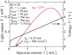
Fig. 2. Current–light output and current–voltage characteristics of fabricated membrane DR laser with a DFB section length of 30 µm.
Download figure:
Standard image High-resolution imageFigure 3 shows the lasing spectrum at a bias current of 1.74 mA (6Ith) under the room-temperature CW (RT-CW) condition. A single-mode operation with a side-mode suppression ratio (SMSR) of 44 dB at a wavelength of 1566 nm was obtained. The difference between the lasing wavelength and the gain peak wavelength was estimated to be 36 nm. The Bragg wavelength detuning effect23) for an improved temperature dependence was expected. Although the longer wavelength mode of the stopband was not clearly observed because of the lack of optical gain, the stopband width of approximately 41 nm (corresponding index-coupling coefficient of approximately 1800 cm−1) was estimated from the devices fabricated from the same wafer. A few peaks inside the stopband show Fabry–Perot resonance between the front facet and front side of the DFB section. The free spectral range (FSR) of 15 nm well agrees with that from the 20-µm-long front waveguide.

Fig. 3. Lasing spectrum under RT-CW condition.
Download figure:
Standard image High-resolution imageFirst, the thermal resistance of the membrane DR laser was investigated theoretically and experimentally. For the theoretical analysis, a typical steady-state heat transfer equation was used for calculation, as described in our previous works.19,20) The membrane laser on a Cu heat sink (width of 11 mm and height of 2 mm) with a 2-µm-thick air gap between the laser and heat sink was assumed as the simulation model. This air gap represented the roughness between the Si substrate and the Cu heat sink. The heat sink temperature was set to 293 K as a boundary condition. The dissipation power Pdiss was defined by the difference between the input power Pin and the light output power Po, and the heat sources of Pdiss-RI2 for 5QWs and RI2 for p-InP were assumed. Here, the assumption that the resistance of the p-InP side cladding region is dominant in the total device resistance24) was used.
The thermal conductivity values in this calculation are listed in Table I; they are the same as those in our previous work.19) Figure 4 shows the cross-sectional temperature distribution of the membrane DR laser with a 30-µm-long DFB section for the input power of 1 mW (corresponding dissipation power Pdiss of 0.94 mW), calculated by a two-dimensional (2D) finite element method (FEM). The temperature increase of 5QWs was 7.2 K. Therefore, the estimated thermal resistance was Rth = ΔT/Pdiss = 7600 K/W. This higher thermal resistance than that of conventional GaInAsP/InP lasers is a result of using cladding materials with low thermal conductivity. For on-chip application, the self-heating effect can be relatively low owing to the low operation current of the membrane laser.19)
Table I. Thermal conductivities [W/(K·m)] used in thermal analysis.
| Material | Thermal conductivity |
|---|---|
| Cu | 400 |
| Au | 320 |
| Si | 158 |
| InP | 68 |
| Ga0.22In0.78As0.81P0.19 (well) | 5.1 |
| Ga0.26In0.74As0.49P0.51 (barrier) | 5.2 |
| Ga0.47In0.53As (Contact layer) | 4.4 |
| SiO2 | 1.4 |
| BCB | 0.29 |
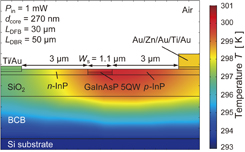
Fig. 4. Simulated cross-sectional temperature distribution of the membrane DR laser.
Download figure:
Standard image High-resolution imageThe thermal resistance was also estimated experimentally. We obtained dλ/dPdiss of 0.52 nm/mW from the slope of the power dissipation dependence of the lasing wavelength, as shown in Fig. 5. Furthermore, dλ/dT of 0.098 nm/K was obtained from the slope of the stage temperature dependence of the lasing wavelength under a pulse condition. As a result, the estimated experimental thermal resistance was Rth = dT/dPdiss = (dλ/dPdiss)/(dλ/dT) = 5250 K/W.
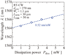
Fig. 5. Lasing wavelength as a function of dissipated power.
Download figure:
Standard image High-resolution imageA difference exists between the obtained theoretical and experimental values. This is because the thermal diffusion to the passive waveguide section and three-dimensional (3D) FEM calculation are required to obtain accurate results. Although the device had a relatively high thermal resistance because of the 2-µm-thick BCB bonding layer with low thermal conductivity, the introduction of the thinner BCB layer could reduce the thermal resistance.19,20)
Next, the temperature dependence of the membrane DR laser was measured. Figure 6 shows the current-light output characteristics for various temperatures. From the results, a 90 °C CW operation with a sub-mA threshold current was obtained for the first time. The improved temperature dependence compared with that of the previously reported device16) can be attributed to the introduction of the Bragg wavelength detuning technique.23) The temperature dependence improvement could be expected by increasing the lasing wavelength at room temperature for the gain peak wavelength.
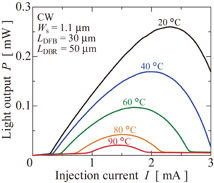
Fig. 6. Current–light output characteristics for various temperatures.
Download figure:
Standard image High-resolution imageThe temperature dependences of the threshold current Ith and the differential quantum efficiency ηdf were expressed by25)


where ΔT is the temperature increase, Ith0 is the threshold current without self-heating, T0 is the characteristic temperature for the threshold current, T1 is the characteristic temperature for the differential quantum efficiency, and ηdf0 is the differential quantum efficiency without self-heating.
Figure 7 shows the threshold current and differential quantum efficiency as a function of temperature. In the temperature range from 20 to 50 °C, the characteristic temperatures T0 of 84 K and T1 of 114 K were obtained. Because these values are higher than typical values for GaInAsP/InP lasers, the Bragg wavelength detuning contributed to the improvement of the temperature dependence. To realize CW operation at a temperature of more than 100 °C, both the reduction in thermal resistance and the improvement of characteristic temperatures were required. Further increase in the amount of Bragg wavelength shift can improve the characteristic temperature. Finally, lasing spectra for various temperatures were measured, as shown in Fig. 8. Single-mode lasing with an SMSR of more than 40 dB was obtained up to 80 °C.

Fig. 7. Threshold current and external differential quantum efficiency as functions of temperature.
Download figure:
Standard image High-resolution image
Fig. 8. Lasing spectra for various temperatures.
Download figure:
Standard image High-resolution image
In conclusion, the thermal properties of a membrane DR laser were described in this paper. The thermal resistance was theoretically and experimentally estimated to be 7600 and 5250 K/W, respectively. The device with a 30-µm-long DFB section realized a 90 °C CW operation with a sub-mA threshold current. An SMSR greater than 40 dB up to 80 °C was demonstrated. These results show the potential of the membrane DR laser for on-chip application.
Acknowledgments
The authors would like to thank Professors S. Akiba, T. Mizumoto, M. Asada, Y. Miyamoto, and M. Watanabe of the Tokyo Institute of Technology for their fruitful discussions. This work was supported by JSPS KAKENHI Grant Numbers 15H05763, 25709026, 15J04654, 15J11776, and 16H06082, and JST-CREST.