

Abstract
The high-external differential quantum efficiency operation of a GaInAsP/InP membrane distributed-reflector laser bonded on a Si substrate was achieved by adopting a short cavity design and reducing the waveguide loss and differential resistance. A threshold current of 0.21 mA, an external differential quantum efficiency of 32% for the front-side output, and a power-conversion efficiency of 12% were obtained with a 32-µm distributed feedback section length, a 50-µm distributed-Bragg-reflector section, and a 0.8-µm stripe width. A side-mode suppression ratio of 41 dB was obtained at a bias current of 1 mA.
Export citation and abstract BibTeX RIS

Content from this work may be used under the terms of the Creative Commons Attribution 4.0 license. Any further distribution of this work must maintain attribution to the author(s) and the title of the work, journal citation and DOI.
This article was made open access on 22 December 2017
Remarkable progress has been made in transistor technology, in accordance with the scaling law.1) However, electrical interconnects in global wire layers continue to experience RC delay and Joule heating problems.2,3) Therefore, the introduction of high-speed and ultra-low power consumption optical communication for on-chip interconnections is attracting attention.2–4) The available transmitter energy for on-chip optical interconnections is assumed to be less than 100 fJ/bit,5) implying that the power consumption should be less than 1 mW at a 10-Gbps data-transmission speed in an on-chip optical interconnection system; thus, an ultra-low power consumption laser is crucial. We estimate that the light output should be greater than 0.16 mW at 10 Gbps with error-free operation, under the assumption of a −13-dBm (50 µW) minimum receivable power for a PIN photodiode, for a bit-error rate (BER) of 10−9 and a link budget of 5 dB.6) Further, assuming a light-source bias voltage of approximately 1 V, the light output should be greater than 0.16 mW at a bias current of 1 mA.
Low-power consumption lasers, such as vertical-cavity surface-emitting lasers (VCSELs),7–9) microdisk lasers,10,11) and photonic crystal lasers (PC-LDs),12–14) have been extensively studied. VCSELs are widely used in short-reach transmissions and supercomputer optical interconnects; however, in-plane integration schemes, such as 45° total reflection mirrors with waveguides, are needed for the on-chip optical interconnects.15) An extremely low energy cost of <5 fJ/bit was demonstrated using a PC-LD and an avalanche photodiode, which requires a bias voltage of a few tens of volts;14,16) however, the energy cost on the receiver side is far higher than that for the transmitter laser.
To realize a transmitter laser with a low threshold current and high-efficiency operation for an on-chip light source, we proposed semiconductor membrane distributed-feedback (DFB) and distributed-reflector (DR) lasers. The semiconductor membrane structure consists of a thin semiconductor core layer sandwiched between low-refractive index dielectric materials or air. Therefore, the optical confinement factor of the active layers is enhanced by a factor of approximately three compared with that for a conventional double-heterostructure laser.17) Because this strong optical confinement effect enhances not only the modal gain but also the index-coupling coefficient of the gratings in the DFB and distributed-Bragg-reflector (DBR) structures, low-threshold current operations and small-footprint devices can be realized.18) Thus, the membrane laser not only is a compact and low-power consumption laser similar to VCSELs, microdisk lasers, and PC-LDs, but also has the great advantage of a high light output-coupling efficiency to in-plane waveguides owing to the edge emitting laser structure. We had demonstrated low-threshold current (0.2–0.3 mA) membrane DFB lasers; however, the external differential quantum efficiency for an output from the front side was <12%.19,20) A 10-Gbps direct modulation of the membrane DFB laser with a BER of 10−9 was achieved at a bias current of 1 mA.20)
To increase the external differential quantum efficiency for the front-side output, we realized a membrane DR laser consisting of a DFB section, with a DBR at its rear. We obtained a threshold current as low as 0.25 mA (threshold current density of 1.2 kA/cm2) and an external differential quantum efficiency of 11% from a front waveguide, with a light output ratio of 6.7 between the front and the rear, using DFB and DBR section lengths of 30 and 90 µm, respectively.21) Then, after adjusting the grating period of the DBR section, a low threshold current of 0.29 mA (threshold current density of 880 A/cm2) and a high external differential quantum efficiency of 23% from the front side were obtained using DFB and DBR section lengths of 30 and 50 µm, respectively.22) However, the light output power at a bias current of 1 mA was 0.12 mW, which was insufficient for the aforementioned condition of the light source for on-chip applications.
Herein, we report a membrane DR laser that exhibits a low threshold current and the highest external differential quantum efficiency ever reported for a membrane laser. By adopting a lower doping concentration of the p-InP side cladding layer and a shorter distance between the p-side electrode and the active region than those of previous work,22) the low differential quantum efficiency due to the high waveguide loss was resolved. A threshold current of 0.21 mA, an external differential quantum efficiency of 32% from the front facet, and a power-conversion efficiency of 12% were obtained. A light output higher than 0.16 mW was obtained at a bias current of 1 mA.
The structure of the fabricated membrane DR laser is shown in Fig. 1(a). This device was fabricated using the same initial wafer used in our previous work,22) which consisted of five GaInAsP quantum wells sandwiched by InP optical confinement layers with a total thickness of 270 nm. After the first selective-area regrowth of the GaInAsP passive waveguide with a bandgap wavelength of 1.22 µm, using organometallic vapor-phase epitaxy (OMVPE), the n- and p-InP side cladding layers were separately regrown to form a lateral-current-injection structure.23) Compared with the previous work,22) the doping concentration of the p-InP side cladding layer was reduced from 2 × 10¹⁸ to 5 × 1017 cm−3 in order to reduce the optical absorption loss from 42 to 22 cm−1.24) Next, a 1-µm-thick SiO2 cladding layer was deposited, and the III–V wafer was bonded to the Si substrate using benzocyclobutene (BCB). The BCB thickness was reduced from 2 µm to approximately 500 nm in order to reduce the thermal resistance.25)
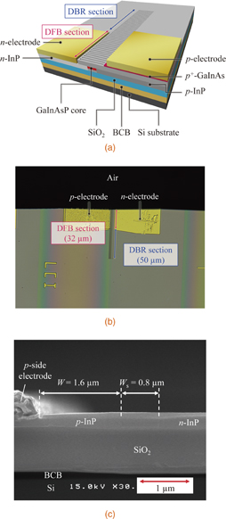
Fig. 1. (a) Schematic of the membrane DR laser, (b) photomicrograph of the fabricated device, (c) cross-sectional SEM view of the fabricated device.
Download figure:
Standard image High-resolution imageBecause the reduction of the doping concentration reduces the optical absorption but increases the series resistance between the p-side electrode and the active region, the distance between the edge of the p-side electrode and the edge of the active section was reduced from 3 µm (in our previous work) to 1.6 µm, to compensate for the resistance increase due to the effect of the lower doped p-InP side cladding layer. After evaporating the p- and n-side electrodes, a 60-nm-deep surface grating was formed by wet chemical etching, where the grating coefficient was expected to be approximately 1,800 cm−1. Figure 1(b) shows a photomicrograph of the fabricated device. The DFB active section length, LDFB, and the DBR passive section length, LDBR, were 32 and 50 µm, respectively. This DBR length can provide a reflectivity higher than 95%.21) The front facet was formed by cleaving. Figure 1(c) shows a cross-sectional scanning electron microscopy (SEM) image of the fabricated device. The stripe width, Ws, and the distance between the edges of the p-side electrode and the active section, W, were 0.8 and 1.6 µm, respectively.
Figure 2 shows the current–light (I–L) and current–voltage (I–V) characteristics of the device shown in Fig. 1 under room-temperature continuous-wave operation. The periods of both the DFB and DBR gratings were set as 298 nm, to match the Bragg wavelength in both the regions. A threshold current, Ith, of 0.21 mA, corresponding to a threshold current density, Jth, of 820 A/cm2, and an external differential quantum efficiency, ηdf, of 32% for the front-side output were obtained. To our knowledge, ηdf = 32% is the highest value reported thus far for membrane-type DFB/DR lasers,19–22,26,27) and among the previously reported membrane DFB and DBR lasers, the present laser exhibited the lowest threshold current and highest differential quantum efficiency. Moreover, the light output from the front side was 0.16 mW at a bias current of 0.84 mA, satisfying the aforementioned condition for a light source for on-chip applications. In addition, a differential resistance of 880 Ω was obtained, which is lower than that in our previous work.22)

Fig. 2. I–L and V–I characteristics of the fabricated membrane DR laser.
Download figure:
Standard image High-resolution imageThe lasing spectrum of the device at a bias current of 1.0 mA (almost five times Ith) is shown in Fig. 3; single-mode operation at 1,535 nm with a side-mode suppression ratio of 41 dB was observed. The Bragg wavelength of the DFB section was intentionally not detuned from its gain peak wavelength, and the amount of wavelength detuning was estimated to be only 5 nm. The resonant modes in the longer-wavelength side of the stopband were not clearly observed, because they were approximately 40 nm away from the Bragg wavelength and their optical gains were considerably low. The index-coupling coefficient, κi, was estimated to be approximately 1,800 cm−1, according to the stopband width of the other devices fabricated at the same time.
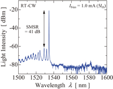
Fig. 3. Lasing spectrum of the membrane DR laser at a bias current of 1.0 mA.
Download figure:
Standard image High-resolution imageFigure 4 shows the power-conversion efficiency, according to the L–I and I–V characteristics shown in Fig. 2. A maximum power-conversion efficiency, ηPCmax, of 12.5% was obtained at a bias current of 0.64 mA, whereas a value of 5.5% was reported for a membrane-type PC-LD.14) A power-conversion efficiency, ηPC, of 12.2% was obtained at a bias current of 0.84 mA when the light output power reached 0.16 mW. In the case of an on-chip membrane photonic integrated circuit, the facet reflection is negligible, and the power-conversion efficiency, ηPC, can be improved to approximately 30% by reducing the distance between the p-side electrode and the active section to 0.8 µm.

Fig. 4. Power-conversion efficiency of the membrane DR laser. The maximum power-conversion efficiency, ηPCmax, of 12.5% was obtained at a bias current of 0.64 mA, and the power-conversion efficiency at an output power of 0.16 mW (I = 0.84 mA) was 12.2%.
Download figure:
Standard image High-resolution imageThe DFB section length dependence of the threshold current of the membrane DR laser with a one-side cleaved facet was calculated, as shown in Fig. 5(a); a threshold current of 0.11 mA can be obtained for a DFB section length of 32 µm, which is approximately 0.1 mA lower than that obtained in the experiment. This discrepancy is attributed to the leakage current through the interface between the active and passive waveguide sections. Thus, the introduction of a current-blocking trench22) is essential for reducing the threshold current. On the other hand, as observed in Fig. 5(b), the external differential quantum efficiency of 32% agrees well with the theoretical value of 36%.

Download figure:
Standard image High-resolution image
Fig. 5. Calculated DFB section length dependences of the (a) threshold current and (b) external differential quantum efficiency from the front facet.
Download figure:
Standard image High-resolution image
In conclusion, we demonstrated the low-threshold current and high-external differential quantum efficiency operation of a membrane DR laser for on-chip optical interconnections. A threshold current of 0.21 mA was obtained for DFB and DBR section lengths of 32 and 50 µm, respectively. The 32% external differential quantum efficiency for the light output from the front facet agreed well with the theoretical value. Additionally, a maximum power-conversion efficiency of 12% was obtained by reducing the waveguide loss, adopting a lower doping concentration for the p-InP cladding layers, and reducing the differential resistance by shortening the distance between the p-side electrode and the active section. Further, the power-conversion efficiency was increased by up to 30% by reducing the distance between the p-side electrode and the active section.
Acknowledgments
The authors thank Professors M. Asada, Y. Miyamoto, T. Mizumoto, and S. Akiba of the Tokyo Institute of Technology, Tokyo, Japan, for the fruitful discussions and comments. This work was supported by the JSPS KAKENHI Grant Numbers 15H05763, 17H03247, 15J04654, 15J11776, and 16H06082 and also by the JST grants JST-CREST (JPMJCR15N6) and JST-ACCEL (JPMJAC1603).