
Abstract
We have fabricated high-density superatom-like Si–Ge-based quantum dots (Si-QDs with Ge core) and studied their luminescence properties. Electroluminescence was observed from the Si-QDs with Ge core at room temperature in the near-infrared region by the application of square-wave pulsed bias of ±1 V at 500 kHz, which was attributed to radiative recombination between quantized states in the Ge core with deep potential well for holes caused by field-effect-induced alternate electron/hole injection from the substrate. The results lead to the development of Si-based light-emitting devices that are highly compatible with ultra-large-scale integration processing, which was found difficult to realize in silicon photonics.
Export citation and abstract BibTeX RIS

Content from this work may be used under the terms of the Creative Commons Attribution 4.0 license. Any further distribution of this work must maintain attribution to the author(s) and the title of the work, journal citation and DOI.
Si and Ge are indirect transition semiconductors.1) However, when the size is reduced to nanometer-scale, these materials show pseudo-direct transition properties.2,3) Therefore, Si-based quantum dots (QDs) have drawn significant attention as active elements in various optical and electronic applications including solid-state quantum computation.4–10) In particular, light emission from Si-based nanostructures including Si- and Ge-QDs has stimulated considerable interest in the field of silicon-based photonics because of the potential to combine photonic processing with electronic processing on a single chip.11–17) The quantum confinement effect leads to enormous increase in the light emission efficiencies of Si- and Ge-QDs. However, for further improving the light emission efficiency and stability, considerable efforts have been made using different approaches that include not only the confinement of injected carriers, but also the use of strained structures and impurity doping. Therefore, we focused on a superatom-like Ge-core/Si-shell QD structure as defect control can be established at interfaces between Si and SiO2. In our previous study, we reported the formation of Si-QDs with Ge core on ultrathin SiO2 layers by alternately controlling the thermal decomposition of SiH4 and GeH4. The unique charge storage characteristics of an individual Si-QD with Ge core, which confirmed type II energy band alignment between the Si clad and Ge core being regarded as a superatom.18)
More recently, we also demonstrated photoluminescence (PL) from the Si-QDs with Ge core, where PL signals had clearly shifted towards high energies with decreasing core size.19,20) In addition, the observed PL spectra were deconvoluted into four main components originating from radiative recombination of photogenerated carriers through quantized states of Si-QDs with Ge core.21) In the present work, based on our recent studies, we designed and fabricated a light-emitting device containing Si-QDs with Ge core embedded in a SiO2 layer similar to a floating gate structure, in which both the electron and hole are injected into the QDs from a p-type Si substrate, and their luminescence characteristics were evaluated at room temperature.
After conventional wet-chemical cleaning steps, ∼2.0-nm-thick SiO2 layer was grown on p-Si(100) by oxidation in dry O2 ambient at 1000 °C. The SiO2 layer thus prepared was slightly etched back in a 0.1% HF solution to terminate the SiO2 surface with Si–OH bonds. After that, Si-QDs with an areal density as high as 2.0 × 1011 cm−2 were formed on the thermally-grown SiO2/p-Si(100) by controlling the early stages of low-pressure chemical vapor deposition (LPCVD) using pure SiH4 at 560 °C. Subsequently, highly selective depositions for the Ge core and Si cap on pre-grown Si-QDs were carried out by thermal decomposition of 10% GeH4 diluted with H2 and pure SiH4, respectively. Afterwards, radical oxidation was carried out using 40% O2 diluted with Ar under 13.3 Pa at 500 °C to cover the dot surface conformally with ∼2.0-nm-thick SiO2 layer. By repeating this process cycle three times, a threefold stacking of the Si-QDs with Ge core embedded in the SiO2 network was formed. For the fabrication of light-emitting device structure, an approximately 7.0-nm-thick SiO2 layer was grown as a blocking oxide by inductively-coupled remote plasma-enhanced chemical vapor deposition using SiH4 and excited O2/Ar at a substrate temperature of 500 °C. Finally, Al/Au top and back electrodes were fabricated by thermal evaporation, where the area of top-electrode was ∼13.5 mm2 and that of the back-electrode was ∼25.0 mm2 provided with an aperture.
The formation of high-density Si-QDs with Ge core was confirmed by atomic force microscopy (AFM) measurements at each process step, as shown in Fig. 1. From the size and distribution of the dots observed in the AFM images, an average dot height of 11.1 nm was deduced including the Ge core (5.7 nm). The dot density remained unchanged after the Ge-core deposition and after Si-clad deposition, while the dot height increased by 5.7 nm after Ge deposition and by 2.3 nm after the Si-clad deposition. The results confirm selective deposition of Ge on pre-grown Si-QDs with an areal dot density as high as 2.0 × 1011 cm−2 and subsequent selective Si-clad formation. In addition, Raman scattering spectra of the threefold stacked Si-QDs with Ge core indicate that compositional mixing hardly occurs at the Si/Ge interfaces during sample preparation as verified from the relative intensity of Si–Ge phonon mode with respect to Si–Si and Ge–Ge phonon modes (not shown).
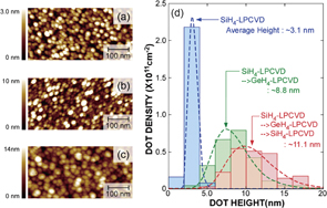
Fig. 1. Typical AFM topographic images: (a) Pre-grown Si-QDs. (b) After Ge deposition. (c) After Si-cap formation. (d) Dot height distribution evaluated from the AFM images.
Download figure:
Standard image High-resolution imageWhen the threefold stacked Si-QDs with Ge core was excited using a semiconductor laser of wavelength 976 nm at an input power of 0.33 W/cm2, a stable PL signal was detected in the energy region between 0.68 and 0.88 eV at room temperature, as shown in Fig. 2(a). Spectral analysis using Gaussian curve-fitting method revealed that the observed PL spectrum can be deconvoluted into four main components, with peaks at 0.70 (Comp. 1), 0.75 (Comp. 2), 0.80 (Comp. 3), and 0.83 eV (Comp. 4). The synthetic spectrum of the four components coincides with the measured spectrum with a fitting error of ∼6%. The full width at half maximum (FWHM) values of the deconvoluted components were 50 meV for Comp. 1–3 and 30 meV for Comp. 4, which can be understood as due to a size variation in the Ge core. From Fig. 1(d), the Ge core height at half maximum of the Ge core height distribution was estimated to be 2.9 and 6.9 nm on either sides of the peak. It was reported that, as the average Ge core height decreased from 7 to 3 nm, the average PL peak energy changed by about 30 meV, which is close to the FWHM value of the deconvoluted components.20) Although the Si clad acts as a shallow potential well for electrons in type II energy band alignment scheme, an electron wave function in the Si clad penetrates into the Ge core. Therefore, it is likely that Comp. 1 is associated with radiative recombination between the electron quantized state in the Si clad and the hole quantized state in the Ge core as discussed in Ref. 21. Comp. 2 is attributed to recombination through the first quantized states of the conduction and valence bands of the Ge core. In addition, radiative transitions between the higher order quantized states in the conduction and valence bands of the Ge core are likely to be responsible for the high-energy Comps. 3 and 4. Further, on application of continuous square-wave pulsed bias of ±1.0 V and over with a duty ratio of 50% at 500 kHz, an EL signal was observed from the backside of the light-emitting device structure with the threefold stacked Si-QDs with Ge core through the c-Si substrate at room temperature. This is shown in Fig. 2(b). During the EL measurements, the top side of the light-emitting device was illuminated with cold light from a 100-W halogen lamp in the 100–800 nm wavelength region through a fiber-optic line equipped with an infrared filter. This helps to generate electrons in the p-Si substrate in the peripheral region of the top-electrode which acts as a virtual source of minority carriers in a manner similar to the source electrode in MOS transistors. Note that the top-electrode shields the QDs from the cold light to prevent photoexcitation and the PL component induced by cold light illumination in the peripheral region of the top-electrode was subtracted from the observed spectra. The observed EL can be explained by radiative recombination through quantized states of the Si-QDs with Ge core caused by alternate electron/hole injection from the p-Si(100). This is because, under cold light illumination, photogenerated electrons in the peripheral region of the area masked with the Al/Au top electrode flow into the inversion region formed below the top electrode and respond to the pulsed bias even at high frequencies. More specifically, the peripheral region with light illumination serves virtually as a source of carriers.22) It may be noted that the observed EL spectra can also be deconvoluted into four components whose peak energies and FWHM values are the same as those of the corresponding components in the PL signal shown in Fig. 2(a). In addition, no significant change in the peak position was observed with increase in applied bias. The integrated EL intensities of all the components together and component-wise are plotted as a function of square-wave bias in Figs. 3(a) and 3(b), respectively. When the applied bias was increased, the integrated EL intensity increased exponentially in all cases except in Comp. 1, which tended to saturate at ±2.0 V. It was also noted that Comp. 4 was hardly detected at applied bias below ±3.0 V. At ±2.0 V, the recombination through the lowest quantized levels, namely the electron quantized state in the Si clad and the hole quantized state in the Ge core (Comp. 1), was more dominant than the recombination through the first and second quantized states in the conduction and valence bands of the Ge core (Comps. 2 and 3). Comp. 4 appeared at ±3.0 V and at higher bias voltage, which is consistent with the radiative transitions between the higher order quantized states of the Ge core, thus implying that photogenerated electrons and holes were injected into higher order quantized states.

Download figure:
Standard image High-resolution image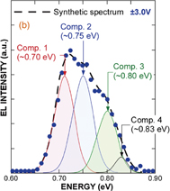
Fig. 2. Room temperature (a) PL spectra. (b) EL spectra of threefold stacked Si-QDs with Ge core and their deconvoluted spectra.
Download figure:
Standard image High-resolution image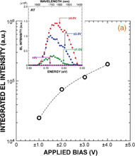
Download figure:
Standard image High-resolution image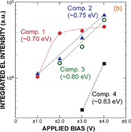
Fig. 3. Integrated EL intensities of: (a) All components. (b) Each component, as function of applied bias. Intensity was evaluated by spectral analysis using a Gaussian curve-fitting method. EL spectra obtained at different applied bias are shown in the inset.
Download figure:
Standard image High-resolution imageWe also evaluated the EL spectra under the application of square-wave bias at different low-voltages (VL) at a constant high-voltage (VH) of 4.0 V and a duty ratio of 50% at 500 kHz, where the square-wave voltage was applied to the back-electrode with respect to the top-electrode. The observed EL spectra could be deconvoluted into four components whose peak energies and FWHM values are the same as the PL and EL spectra discussed in Figs. 2(a) and 2(b). The integrated EL intensity of each component was deduced from the EL spectra and plotted as a function of VL in Fig. 4. All the components were detected even at a low VL value of −1.0 V, and the EL intensity of each component rose exponentially with increase in the |VL|. Further, no significant changes were observed in the spectral shape, namely peak position and FWHM. The observed EL is ascribed to electron injection in the QDs during application of low-voltage bias (VL) and successive recombination with holes stored in the Ge core during the VH application reflecting the deep potential well as schematically illustrated in the inset of Fig. 4. In this bias condition, the electron injection rate during the application of VL is enhanced due to the positive charges created in the QDs by hole injection in the Ge core, which facilitates EL at low negative bias. It should be noted that the EL spectral shape was drastically changed when the EL spectra were measured at different VH with a constant VL of −4.0 V. Figures 5(a) and 5(b) show the normalized EL spectra of a light-emitting device with threefold stacked Si-QDs with Ge core as a function of energy measured at different VH (VL was kept constant at −4.0 V) and integrated EL intensity of each component (extracted from the spectral deconvolution where peak energies and FWHM values were kept the same as those of the PL signal) as a function of |VH|, respectively. Obviously, with an increase in the VH, an increase in the EL intensity of the components on the high-energy side becomes dominant, although Comp. 1 is dominant at 0 V. In addition, a plateau was observed in the EL intensity of each component between VH values ranging from 2.0 to 3.0 V. These results can be interpreted in terms of hole injection which can be caused even at 0 V by the negative charge of electrons stored in the Si-QDs with Ge core at −4.0 V. This is schematically illustrated in the band energy diagram in Fig. 6(a). Hole injection from the p-Si(100) to the Ge core during VH application plays a major role in the radiative recombination of injected electrons and holes. In the bias (VH) range from 0 to 2.0 V, the EL intensity increased with bias voltage which is attributed to an increase in the hole tunneling rate. At bias voltages between 2.0 and 3.0 V, electrons in the QDs are partially extracted before radiative recombination occurred with injected holes [Fig. 6(b)] resulting in a plateau in the EL intensity curve. With further increase in VH (3.0 V and above), electron injection becomes a rate-limiting factor, as shown in Fig. 6(c); here, stable EL process becomes dominant and EL intensity increases at negative bias while EL intensity reduces due to electron extraction from the QDs at positive bias. It is hoped that the above findings which resulted from the introduction of a Ge core into the Si-QDs (pseudo-superatom structure) will help to realize Si-based optoelectronic devices capable of generating a stimulated radiation of narrow bandwidth emission characteristics at low-voltage bias and high emission intensities resulting from a highly efficient carrier recombination process.

Fig. 4. Integrated EL intensity of each component deduced from EL spectra measured at different square-wave bias voltages (VL), where VH was kept constant at 4.0 V. Inset shows energy band diagram of the Si-QDs with Ge core illustrating electron injection under negative bias application after hole charging at 4.0 V.
Download figure:
Standard image High-resolution image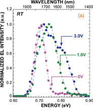
Download figure:
Standard image High-resolution image
Fig. 5. (a) Normalized EL spectra as a function of energy measured at different VH in square-wave bias, where VL was kept constant at −4.0 V. (b) Integrated EL intensity of each component as a function of VH at VL = −4.0 V.
Download figure:
Standard image High-resolution image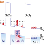
Download figure:
Standard image High-resolution image
Download figure:
Standard image High-resolution image
Fig. 6. Schematic of the energy band diagrams of the Si-QDs with Ge core fabricated on SiO2/p-Si(100). (a) Hole injection at 0 V. (b) Electron emission from the dots to the substrate at bias voltages 3.0 V and above. (c) Electron injection from the substrate to the dots at −4.0 V after the application at a voltage of 3.0 V and above.
Download figure:
Standard image High-resolution image
In summary, we have demonstrated stable EL in the near-infrared region from a light-emitting device consisting threefold stacked Si-QDs with Ge core with an areal density of 2.0 × 1011 cm−2 under pulsed bias operation. When square-wave bias voltages (VH) were applied at a constant bias voltage VL = −4.0 V, hole injection resulted for 0 < VH < 2.0 V and electron injection for 3.0 V and are major EL rate-limiting factors. The formation of Si-QDs with Ge core is helpful in realizing high-efficiency EL devices. Our results imply that superatom-like Si–Ge-based QDs show great promise in optoelectronic device applications.
Acknowledgment
This work was supported in part by Grant-in-Aid for Scientific Research (S) No. 15H05762 of MEXT Japan.