Abstract
In X-ray grating interferometry, the fabrication of thick transmission gratings with pitches of several micrometers has been a key subject. We report on a metallic glass imprinting technique for fabricating an interferometer grating. We successfully fabricated an 8-µm-pitch, 10-µm-thick grating (26 mm2) made of Pd42.5Ni7.5Cu30P20 metallic glass by using the technique, and as a demonstration we also performed X-ray phase imaging with the grating. The technique can be applied to fabricate not only X-ray but also neutron gratings potentially at high production rates and low costs and is expected to be widely used in the near future.
Export citation and abstract BibTeX RIS

Content from this work may be used under the terms of the Creative Commons Attribution 4.0 license. Any further distribution of this work must maintain attribution to the author(s) and the title of the work, journal citation and DOI.
This article was made open access on 16 September 2015
X-ray grating interferometry, which is one of several X-ray phase imaging techniques1–3) used for high-sensitivity X-ray imaging, has been spotlighted in the past decade.4–14) This novel X-ray imaging technique has the advantage that it can use a compact low-brilliance laboratory X-ray source, and it is now increasingly applied in many fields including medicine, biology, material sciences, and industry. Neutron grating interferometry, which makes it possible to realize neutron phase imaging, has also been proposed and spotlighted recently; it can, for example, provide complementary structural information including details of magnetic domains.15–22)
In X-ray and neutron grating interferometries, fabrication of thick, large-area transmission gratings has been a key subject. Both these grating interferometers consist of two or three gratings, and a self-imaging phenomenon called the "Talbot effect"23) is used. For a self-image to be visible, one of the gratings has to be illuminated by an X-ray or neutron beam whose spatial coherence length is comparable to or larger than the pitch of the grating. As a result, the pitch of the grating has to be typically less than several micrometers. In addition, the thicknesses of the gratings used in the interferometers has to be more than a few micrometers to effectively interact with X-rays or neutrons. Particularly, an absorption grating that is superimposed on the self-image has to be sufficiently thick to generate a Moiré pattern. In order to fully use a large-area X-ray or neutron beam, large-area gratings are also desired. For these reasons, thick, large-area gratings with pitches of less than several micrometers and thicknesses of more than a few micrometers (at least more than several micrometers for an absorption grating) are typically required.
Although it is difficult to fabricate such a thick, large-area grating, several approaches have so far been reported for X-ray24–31) and neutron15,32,33) grating interferometers. For X-ray grating interferometers, gratings are typically made of heavy elements (e.g., gold), which interact with X-rays effectively. So far, electroplating has been widely used to fabricate such gratings and gratings of 10 × 10 mm2 in size have already been realized, but the process is time consuming and requires a very uniform pattern because the increase in local thickness of electroplated material during the electroplating process makes the local plating current higher, enhancing the nonuniformity of its thickness. For these reasons, it is generally not easy to fabricate large-area (and especially, high-aspect-ratio) gratings by electroplating with high yield ratios and low costs. In contrast, gadolinium is used for neutron absorption gratings because it absorbs neutrons most effectively. However, the micro-fabrication process for gadolinium is not well established, and the gadolinium gratings reported previously are not sophisticated.
In this paper we report on another approach — a metallic glass imprinting technique for fabricating transmission gratings for X-ray grating interferometers. Metallic glass, i.e., an amorphous material, can be formed by rapid solidification of an alloy melt to room temperature (RT). One characteristic of this material is the existence of a supercooled liquid (SCL) region beyond the glass transition temperature, which located at ∼50–60% of the melting point, upon heating. In the SCL state, metallic glass exhibits Newtonian viscous flow,34,35) whereby the viscosity decreases to as low as 105–108 Pa·s.36) Owing to the near-net-shape-forming ability, metallic glass has been applied for patterning various shapes on nano- and micrometer scales by surface imprinting.37–40) This imprinting technique should be potentially suitable for fabrication of gratings for X-ray (or neutron) grating interferometers because it requires neither a long time nor a quite uniform pattern and its simple process can allow for fabrication of large-area gratings at high production rates and low costs.
Among the number of glass-forming alloys, in the present study we selected a Pd42.5Ni7.5Cu30P20 (at.%) glass owing to its excellent glass-forming ability and high thermal stability of the SCL,41) as well as its relatively large interaction with X-rays expected by the Pd constituent. We successfully fabricated an 8-µm-pitch, 10-µm-thick a Pd42.5Ni7.5Cu30P20 metallic glass grating by using the imprinting technique. As a demonstration, we also performed X-ray phase imaging by using the grating and successfully obtained a differential phase image.
The process of fabricating the metallic glass grating is shown in Fig. 1. First, a Si grating pattern (mold) with a pitch of 8 µm and a depth of 10 µm was prepared by inductively coupled plasma (ICP) etching [Fig. 1(a)]. Next, a 10 × 15 mm2 ribbon of the a Pd42.5Ni7.5Cu30P20 metallic glass (9.33 g/cm3)42) was heated to 330 °C and pressed into the mold under a pressure of 40 MPa for 100 s in an inactive ambient gas [Fig. 1(b)]. After removal of the Si mold by etching in a sodium hydroxide aqueous solution followed by rinsing in demineralized water, a copy of the grating pattern was formed on the metallic glass [Fig. 1(c)]. Finally, the back side of the metallic glass was thinned and polished to reduce loss of X-ray intensity from absorption and scattering [Fig. 1(d)].
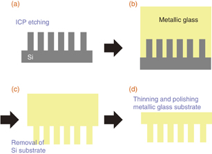
Fig. 1. Metallic glass grating fabrication process. (a) First, a Si grating pattern (mold) is prepared by ICP etching. (b) A ribbon of metallic glass is heated to 330 °C and pressed into the mold under a pressure of 40 MPa under an inactive gas. (c) A copy of the grating pattern is then formed on the metallic glass after the removal of the Si mold. (d) Finally, the back side of the metallic glass is thinned and polished to reduce absorption and scattering of X-rays.
Download figure:
Standard image High-resolution imageA scanning electron microscopy (SEM) image of the Si grating mold fabricated is shown in Fig. 2(a). Figures 2(b)–2(d) show SEM images of the fabricated metallic glass grating from the mold. Figure 2(b) seems to indicate that the metallic glass grating was uniformly fabricated over a wide area. Figures 2(c) and 2(d) show that an 8-µm-pitch, 10-µm-thick metallic glass grating was successfully realized over a local area. In the section image in Fig. 2(d), it can be seen that the surface of the Si mold was faithfully copied; even scallops on the side walls of the grooves were copied to the metallic glass.
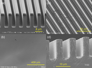
Fig. 2. (a) SEM image of a section of a Si grating pattern (mold) with a pitch of 8 µm and a depth of 10 µm fabricated by ICP etching. (b) Wide-area, (c) magnified, and (d) magnified section SEM images of a copied metallic glass grating fabricated by using the process of Fig. 1.
Download figure:
Standard image High-resolution imageBecause the SEM image shown in Fig. 2(d) provides information on only a local area and does not ensure that the grating pattern is copied successfully over a wide area, we constructed an X-ray grating interferometer with the metallic glass grating to check its global performance. The experimental setup is shown in Fig. 3. We used a micro-focus X-ray source (Hamamatsu Photonics L9181S) with a tungsten target. The tube voltage and tube current of the X-ray source were set to be 50 kV and 120 µA, respectively. A 5.3-µm-pitch Au phase Ronchi grating (G1) with a thickness of 2.7 µm, fabricated on a 200-µm-thick Si substrate, was located at a distance of 838 mm from the X-ray source. The 8.0-µm-pitch metallic glass grating fabricated (G2) was then located at a distance of 427 mm from the phase grating, corresponding to a Talbot order of 0.5. We used a CCD-based X-ray image detector with an effective pixel size of 18 µm (Spectral Instruments 1000 series), having a 40-µm-thick Gd2O2S: Pr scintillator on a 1 : 2 fiber coupling connected to a CCD chip of 4096 × 4096 pixels (9 µm/pixel).
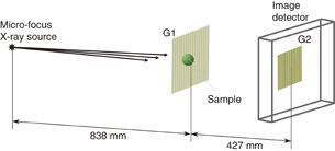
Fig. 3. Experimental setup of an X-ray grating interferometer with the metallic glass grating fabricated.
Download figure:
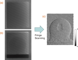
Standard image High-resolution imageFigure 4(a) shows a rotation Moiré image without a sample. The fact that the Moiré fringe obtained is hardly distorted in the area (4.7 × 5.6 mm2) shown in the figure reflects the uniformity of the pitch and the very small lattice distortion (∼10−3 in the direction of its period) of the metallic glass grating. The visibility of the Moiré patterns was (2.1 ± 0.1)% over the area. The average value of the visibility was reproduced by a simulation, where we used the measured continuous X-ray spectrum and assumed an X-ray source with an 8.0-µm-FWHM-maximum Gaussian intensity distribution and a 10-µm-thick metallic glass grating with a duty cycle of 0.5 on a 30-µm-thick metallic glass substrate.
Fig. 4. (a) Moiré image obtained by using the metallic glass fabricated (without a sample). (b) Moiré image with a sample (a 2.4-mm-diameter POM sphere with a void inside). (c) Differential phase image of the sample (gray scale: phase of the Moiré fringe).
Download figure:
Standard image High-resolution image
We also performed X-ray phase imaging by using the X-ray grating interferometer as a demonstration. A POM sphere with a diameter of 2.4 mm with a void inside was used as a sample, which was placed just in front of G1 (magnification: 1.66). Figure 4(b) shows a rotation Moiré image with the sample. Figure 4(c) shows a differential phase image of the POM sphere obtained by a 15-step fringe scanning technique43–45) with an exposure time of 10 min for each step. Thus, X-ray phase imaging was successfully performed by using the metallic glass grating.
The technique presented in this paper should be suitable for high-production-rate, low-cost fabrication of gratings for X-ray and neutron grating interferometers. The imprinting technique requires neither a long time nor a very uniform mold pattern, which are both necessary for conventional electroplating. In addition, reuse of the mold should be possible in the case of the imprinting technique, as has already been realized for smaller structures,37–40) whereas molds have not yet been reused in electroplating. Another advantage is that we can select a material from various glass-forming alloys consisting of metallic elements including Pd and Gd, whereas normal imprinting techniques use soft materials consisting of light elements, which are not suitable for either X-ray or neutron gratings. For these reasons, the imprinting technique presented here should be promising for X-ray and neutron grating interferometers in the near future.
In summary, we proposed a metallic glass imprinting process for fabricating gratings for X-ray grating interferometers. A grating pattern with an 8-µm pitch and a 10-µm thickness was copied to the surface of a Pd42.5Ni7.5Cu30P20 metallic-glass ribbon and its back side was thinned and polished. It was confirmed by SEM [Figs. 2(b)–2(d)] and X-ray grating interferometry [Fig. 4(a)] that an 8-µm-pitch, 10-µm-thick metallic glass grating was successfully fabricated in an ∼5 × 5 mm2 area by the imprinting technique. X-ray phase imaging was also performed as a demonstration by using the X-ray grating interferometer, and a differential phase image was indeed realized [Fig. 4(c)].
Acknowledgment
This research was supported by the SENTAN Project of the Japan Science and Technology Agency (JST).