Abstract
We grew crystalline MgB2 thin films using molecular beam epitaxy at a low substrate temperature of 110 °C under an ultrahigh vacuum of about 10−6 Pa. MgB2 thin films were deposited on the (001) surface of a 4H-SiC substrate with an epitaxial Mg buffer layer. Superior crystallinity and surface flatness were confirmed by in situ reflection high-energy electron diffraction and X-ray diffraction measurements. The growth temperature was lower than any in prior reports on superconducting MgB2 thin films. Moreover, we successfully confirmed the occurrence of a sharp superconducting transition at 27.2 K.
Export citation and abstract BibTeX RIS

Content from this work may be used under the terms of the Creative Commons Attribution 4.0 license. Any further distribution of this work must maintain attribution to the author(s) and the title of the work, journal citation and DOI.
MgB2 has significant potential for fabricating highly efficient superconducting devices because of its remarkably high superconducting transition temperature, Tc = 39 K;1) small penetration depth, λ ≃ 40 nm;2) and extremely short electron–phonon scattering time, τe–ph ≃ 3 ps.3) Fabrication of superconducting devices based on MgB2 thin films requires the development of nanofabrication processes and methods for growing high-quality MgB2 thin films. Several research groups have developed techniques for the growth of high-quality MgB2 films, such as the two-step method,4) hybrid physical–chemical vapor deposition,5) and sputtering.6) To fabricate a superconducting thin film, these methods require elevated substrate temperatures (above 700 °C) during deposition or a post-deposition annealing process at temperatures as high as 600–800 °C. High-temperature procedures are, however, not suitable for obtaining a sharp interface between the superconducting MgB2 and insulator layers in multilayer superconducting devices. Nanostructures can be fabricated via a conventional lift-off process only at temperatures lower than 150 °C. Thus, techniques for as-grown synthesis based on low-temperature processes have been developed on the basis of molecular beam epitaxy (MBE),7–10) sputtering,11) and co-evaporation.12) Some studies have attempted to perform low-temperature growth using epitaxial buffer layers with good lattice matching, such as AlN (1.9%),13) TiZr (3.6%),14) and Ti (4.1%).15) The in-plane axis of MgB2 tends to align with that of the buffer layer when the substrate temperature remains low during the entire process. In particular, among these bilayer films, MgB2/Ti films that showed a sharp superconducting transition at Tc = 36 K were obtained by growth at the lowest temperature of 200 °C.15) However, this temperature is higher than the applicable temperature limit for a standard organic resist. Therefore, a lift-off-like process using an inorganic material as a resist,16) Ar ion milling,17) or focused ion beam milling18) has been applied to fabrication of MgB2 nanowire structures. However, the physical dry etching process often severely damages the superconducting film.
In this study, we describe the fabrication of epitaxial MgB2 thin films on a Mg/4H-SiC substrate at a significantly low substrate temperature of 110 °C by the MBE method. We note that the substrate temperature was obtained not by intentional heating, but rather by radiation heating from Knudsen cells (K cells) in the chamber. Therefore, we call this temperature the ambient temperature. Mg has a hexagonal crystal structure with the lattice constants a = 3.2125 Å and c = 5.2132 Å. The lattice mismatch between Mg and MgB2 is thus 4.1%, which is larger than the mismatch values for AlN, TiZr, and Ti. Although good lattice matching is generally effective for epitaxial growth, we note that wetting at interfaces between the buffer layers and the MgB2 layer is also important for epitaxial growth. One can expect good wetting at an interface between the Mg and MgB2 layers. An as-grown film showed a sharp superconducting transition at Tc = 27.2 K.
Thin films of MgB2 were grown by the MBE method. The pressure during the growth process was about 2 × 10⁻⁶ Pa. The elementary materials Mg and B were deposited by the K cells. The temperature of each K cell was stabilized at the set point within ±0.1 °C during deposition. This ensured that each deposition rate was highly stable for the entire duration of film deposition. The (001) surface of a 4H-SiC substrate was used after cleaning in acetone and ethanol for 10 min and blow drying with nitrogen. Before deposition, the 4H-SiC substrate was heated to 1000 °C and kept for an hour in the growth chamber under high vacuum for degassing. It was then cooled to room temperature. The substrate temperature was determined to remain at 110 °C within an accuracy of 5 °C by several irreversible thermolabels placed on the top surface of the substrate holder. It was increased by radiative heating from the K cells, and we did not use the substrate heater for intentional heating. The deposition rate was monitored by a quartz oscillating monitor located below the substrate. We evaluated the deposition rate by monitoring a resonant frequency change at intervals of 1 min to recover a very low rate. We found that the deposition rate thus obtained was well stabilized within ±0.014 Å/min with respect to the deposition rate of 0.7 Å/min. The Mg buffer layer was deposited at a typical deposition rate of 3 Å/min to form a 30-nm-thick film. After deposition of the Mg buffer layer, the MgB2 layer was deposited by co-evaporation of Mg and B. The deposition rate ratio of Mg to B was  , which is the same as the MgB2 stoichiometric ratio. This contrasts sharply with prior reports on MgB2 films, where excess Mg was thought to be necessary to grow MgB2 films. The typical deposition rate and film thickness of the MgB2 layer were 0.7 Å/min and 100 nm, respectively. The surface flatness and crystallinity during deposition were monitored by reflection high-energy electron diffraction (RHEED). The structure of the films was investigated using X-ray diffraction (XRD), and the surface flatness of the films was measured using an atomic force microscope (AFM). The resistivity was measured using the conventional four-probe method.
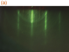
Figures 1(a) and 1(b) show the RHEED patterns for Mg and MgB2, respectively. The RHEED image of Mg shows a sharp streak pattern, indicating epitaxial growth of Mg thin films with good crystallinity and atomic-scale surface flatness. On the other hand, the MgB2 RHEED pattern is spot-like, implying a relatively rough surface. With rotation of the incident direction of the electron beam, both patterns changed, confirming in-plane alignment of the Mg and MgB2 thin films.
Download figure:
Standard image High-resolution image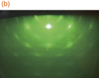
Fig. 1. RHEED images for (a) Mg and (b) MgB2.
Download figure:
Standard image High-resolution imageThe presence of a relatively rough MgB2 film surface as detected by RHEED was directly confirmed by examining the MgB2 AFM image shown in Fig. 2. Although some protuberances appear in the image, we estimate the average surface roughness to be 3.4 nm. Although the origin of these protuberances is not fully understood yet, it is possible that they may result from excess Mg, B, and MgO.

Fig. 2. AFM image of MgB2.
Download figure:
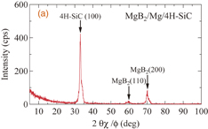
Standard image High-resolution imageFigure 3(a) shows the interplane XRD pattern for MgB2/Mg bilayer films grown on the (001) surface of the 4H-SiC substrate. The (001) and (002) peaks of MgB2 and (002) and (004) peaks of Mg are observed, giving clear evidence of successful growth of MgB2/Mg bilayer thin films. We also observed a contamination peak at around 44°, marked by the † symbol; the origin of this peak has not been identified yet. The exclusive appearance of the (00l) peaks in MgB2 and Mg revealed that the film has a distinct c-axis-oriented structure. The XRD rocking curves for the (002) MgB2 peak and (004) Mg peak are shown in Figs. 3(b) and 3(c), respectively. The full width at half-maximum (FWHM) of the (004) Mg peak (0.25°) is much smaller than that of the (002) MgB2 peak (1.54°). This corresponds to the fact that the RHEED pattern of Mg is noticeably sharper than that of MgB2, as shown in Fig. 1.

Fig. 3. (a) Interplane XRD pattern for MgB2. Substrate peaks are indicated by *. Impurity peak appears at 44°, as indicated by †. Rocking curves for (b) MgB2(002) and (c) Mg(004) peaks.
Download figure:
Standard image High-resolution imageThe grazing-incidence XRD profile for a MgB2/Mg film is shown in Fig. 4(a). The (200) MgB2 peak and the (100) peak of the 4H-SiC substrate are observed, indicating that MgB2 grains were grown with the MgB2[100] ∥ 4H-SiC[100]. Observation of the finite (110) MgB2 peak indicates the existence of unoriented grains. We also determined the degree of epitaxy for the Mg buffer layer by employing Mg[100] ∥ 4H-SiC[100] in grazing-incidence XRD measurements (not shown). Figure 4(b) shows the ϕ-scan pattern of the (103) MgB2 peak. Clear six-fold peaks are observed, consistent with the six-fold symmetry of MgB2. On the basis of the RHEED and XRD patterns, we conclude that we successfully obtained partially epitaxial MgB2 films, although some of the grains are randomly oriented with respect to the in-plane axis.
Download figure:
Standard image High-resolution image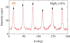
Fig. 4. (a) In-plane XRD pattern for MgB2 and (b) ϕ scan of the MgB2(103) peak.
Download figure:
Standard image High-resolution imageFigure 5 shows the X-ray reciprocal lattice mapping. The (103) MgB2 peak is clearly observed; using the peak position, we determined the MgB2 lattice constants to be a = 3.075 Å and c = 3.576 Å. These results are within 0.4 and 1.5% of the bulk a and c values, respectively, and thus show fairly good agreement with the bulk values. The 0.98° FWHM of the (103) MgB2 peak in the rocking curve was comparable with that of the (002) peak. The average coherent domain size D was estimated as 57 nm by applying the Debye–Scherrer formula D = 0.9λ/β cos θ, where λ is the X-ray wavelength, and β is the FWHM of a diffraction peak in the 2θ scan.
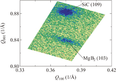
Fig. 5. Reciprocal lattice mapping around the MgB2(103) peak.
Download figure:
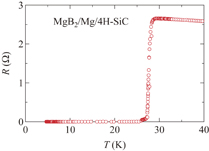
Standard image High-resolution imageThe temperature dependence of the electrical resistance R for MgB2/Mg/4H-SiC is shown in Fig. 6. Below room temperature, R increases with decreasing temperature because of the influence of the semiconducting resistance of the 4H-SiC substrate. Superconductivity appears below Tc = 27.2 K, and the superconducting transition width is relatively narrow, ΔTc = 0.9 K. Annealing is well known to dramatically improve Tc in MgB2. Shibata et al. indicated that the film surface of MgB2 deteriorates in air.18) Therefore, the lower Tc values of our as-grown MgB2 thin films relative to that of the bulk samples are due to the absence of post-deposition-annealing and surface oxidization.
Fig. 6. Temperature dependence of the electrical resistance for MgB2.
Download figure:
Standard image High-resolution image
We grew superconducting MgB2 thin films with a buffer layer of epitaxial Mg on the (001) 4H-SiC substrate surface. We emphasize that this study represents the first time that MgB2/Mg/4H-SiC thin films were fabricated at an ambient temperature lower than 110 °C. To the best of our knowledge, this is the lowest deposition temperature for partial epitaxial growth of MgB2 thin films. The Tc values of the present thin films are comparable to previously reported results; the observed suppression of thin film Tc values is known to be related to the decreased substrate temperature. The presence of the Mg buffer layer is crucial for reducing the epitaxial temperature. MgB2 thin films with relatively good crystallinity and superconducting properties were obtained at a substrate temperature of 110 °C. We note that epitaxial superconducting MgB2 thin films were also obtained without prior annealing of the 4H-SiC substrate. Thus, prior high-temperature annealing is not necessarily required for obtaining a superconducting MgB2 thin film on a photoresist-patterned substrate. We believe that this finding suggests a new process for fabricating nanostructured MgB2 films with the aid of an organic-based lift-off resist. Since the discovery of MgB2, the use of MgB2-based devices in a wide range of possible applications has been limited owing to the absence of conventional techniques for nanoscale structure fabrication. Our new MgB2 thin film growth process is promising for the development of a convenient nanofabrication technique for MgB2 thin films based on a standard lift-off process with a commercial organic resist. We think that our innovative method will strongly affect the expansion of the use of MgB2 materials in future.
Acknowledgments
This study is supported by a Grant-in-Aid for Young Scientists (A) (No. 24684027) and a Grant-in-Aid for Scientific Research (S) (No. 23226019) from the Japan Society for the Promotion of Science (JSPS) and by a special grant for faculty innovation from the Graduate School of Engineering at Osaka Prefecture University.