Abstract
A large output voltage of 0.7 mV at 1 mA charge current is demonstrated for all-metallic nonlocal spin valves using Co2(FeMn)Si Heusler alloy and Cu with a junction area of about 50 nm2. The output is attributed to the junction size reduction as well as to the high spin polarization in the Heusler alloy. An analysis using a one-dimensional model reveals that the spin diffusion length in the Cu layer shows no clear degradation even in the case of a 50 nm2 junction. When the junction is reduced further to 10 nm2, an output voltage of about 10 mV is expected.
Export citation and abstract BibTeX RIS

Content from this work may be used under the terms of the Creative Commons Attribution 4.0 license. Any further distribution of this work must maintain attribution to the author(s) and the title of the work, journal citation and DOI.
This article was made open access on 10 February 2016
For high-density magnetic recording over 2 Tbit/in.2, the total thickness of a read sensor should be reduced to less than 20 nm. However, conventional spin valve sensors cannot meet this specification because of their thick stack of pinned magnetic and antiferromagnetic layers. Nonlocal spin valves (NLSVs), which have a lateral structure and use spin-accumulation effects,1,2) are promising for solving this problem. The pinned/antiferromagnetic layer stack is placed outside the read gap area. The output voltage generated by a pure spin current is also preferable from the standpoints of electric circuit noise and reliability.
One of the challenges for NLSV sensors is the small output voltage. It has been reported that the output (measured by the resistance change) of all-metallic NLSVs using NiFe wire ranges from a value below 1 mΩ (submicrometer junction) to 9 mΩ (50 nm junction).3–9) All-metallic NLSVs using Heusler alloys, which have a higher spin polarization than NiFe, show an output of up to 17 mΩ.10–12) From these results, it is effective to use the Heusler alloys with a reduced junction size for obtaining a high output. However, the reported outputs are still too low for application in read head sensors. NLSVs with a thin MgO layer between ferromagnetic (FM) and nonmagnetic (NM) wires are reported to have a large output of 400 mΩ13) However, a large junction resistance is not suitable for high-density high-speed hard disk drive applications.
In this paper, attempts to increase the output of all-metallic NLSVs are reported. The junction size is reduced to 50 nm. Co2(FeMn)Si (CFMS) polycrystalline Heusler alloys14,15) are used to increase spin polarization. Results are analyzed using a one-dimensional analytical model. The extensibility of this system to recording densities of over 2 Tbit/in.2 is also discussed.
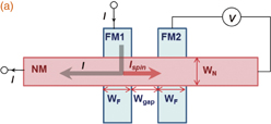
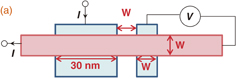
Figure 1(a) shows a layout of a test chip. The widths of the NM wire (WN), FM wires (WF), and gap between the two FM wires (Wgap) were set to the same value. They were changed from 50 to 150 nm. The film stack at the FM/NM junction was Ta (2 nm)/Cu (10 nm)/Co2Fe0.4Mn0.6Si (6–20 nm)/Cu (20 nm). The area around the junction was filled with a SiO2 insulating layer.
Download figure:
Standard image High-resolution image
Fig. 1. (a) Schematic illustration of test chip. NM: nonmagnetic Cu wire; FM: magnetic wire. WN, WF, and Wgap are set to the same value (WN = WF = Wgap). (b) Plan-view SEM image of an NLSV sample. WN = WF = Wgap = 150 nm.
Download figure:
Standard image High-resolution imageFirst, the FM wires were deposited by conventional magnetron sputtering at room temperature on a thermally oxidized Si substrate. The film stack was Ta (2 nm)/Cu (10 nm)/Co2Fe0.4Mn0.6Si (6–20 nm)/Cu (20 nm)/capping. The CFMS layers exhibited a (110)-oriented polycrystalline structure. The composition of the CFMS layer estimated by inductively coupled plasma mass spectrometry (ICP-MS) was Co49Fe10Mn16Si25 in at. %. The CFMS layers were annealed at 290 to 400 °C for 1 h in order to induce the L21 or B2 chemically ordered phase. The thermal stability of our CFMS/Cu films limited the annealing temperature to 400 °C owing to the interdiffusion. We formed two parallel FM wires by nanoimprint lithography and Ar ion milling with a hard mask. After this first patterning step, a SiO2 layer was deposited in order to fill the area surrounding the FM wires. We then etched the SiO2 layer to form a flat surface while partially uncovering the top Cu layer of the FM wires. The SiO2 layers, hard mask layer, and capping layer on the junction area were etched out so that 2–5 nm of Cu remained on the junction. Then, a Cu (25–50 nm) layer was deposited on it without breaking the vacuum in order to obtain a low junction resistance between the FM and NM layers. The Cu layer was then patterned into a wire crossing over the FM wires by the same process as with the FM wires. A plan-view scanning electron microscopy (SEM) image of the fabricated NLSV sample (W = WN = WF = Wgap = 150 nm) is shown in Fig. 1(b).
Cross-sectional transmission electron microscopy (TEM) images of the sample with W = 50 nm are shown in Fig. 2. Figure 2(a) shows a cross section across the two FM wires and Fig. 2(b) shows that across the NM wire. The junction width at the CFMS/Cu interface was about 50 nm, although the junction exhibited a tapered shape. Redeposition of the CFMS layer and oxidation on the side wall of the Cu layer, which degrade the spin diffusion length, were not observed by energy-dispersive X-ray spectroscopy.

Download figure:
Standard image High-resolution image
Fig. 2. Cross-sectional TEM images of a fabricated NLSV sample. WN = WF = Wgap = 50 nm. (a) Cross section across the two FM wires. (b) Cross section across the NM wire.
Download figure:
Standard image High-resolution imageNonlocal magnetoresistance was measured at room temperature as follows. A spin-polarized current from the CFMS1 wire was injected into the Cu NM wire. A pure spin current then flowed through the NM wire from the NM/CFMS1 interface to the CFMS2/Cu interface. The difference in the chemical potential based on the spin configuration (parallel or antiparallel) at the two FM wires was detected as the output voltage at the CFMS2/Cu interface.
Figure 3(a) shows the change in output as a function of annealing temperature for the sample with W = 150 nm. Note that it is difficult to detect ordered B2 and L21 peaks for the (110) orientation by conventional X-ray diffraction. Therefore, the ordered structure was investigated by in-plane TEM diffraction using an electron-beam spot of 1 nm diameter. The schematic TEM diffraction patterns for A2, B2, and L21 structures are shown in Fig. 3(d). At the annealing temperature of 290 °C, an output of around 5 mΩ was obtained. In this case, diffraction spots for the B2 chemically ordered phase were detected [Fig. 3(b)]. When annealed at 400 °C, the output increased to around 10 mΩ, and spots for the L21 chemically ordered phase were detected in half of the investigated grains [Fig. 3(c)]. The twofold increase in the output shown in Fig. 3(a) is attributable to the spin polarization enhancement by the formation of the L21 chemically ordered phase. The output voltage of the polycrystalline CFMS sample annealed at 400 °C was almost the same as that of the single-crystal CFMS annealed at 500 °C.16) This result indicates that the defects in the polycrystalline films may accelerate chemical ordering.

Fig. 3. (a) Change in output as a function of annealing temperature with 150 nm element size. (b, c) Electron diffraction patterns for the film sample at 290 and 400 °C. (d) Schematic TEM diffraction patterns for A2, B2, and L21 structures.
Download figure:
Standard image High-resolution imageThe junction size (W) dependence of the output voltage (ΔV) at 1 mA injection current is shown in Fig. 4 for samples annealed at 400 °C. ΔV increased about 50-fold with decreasing W from 150 to 50 nm. The large ΔV distribution for samples with W of 55–85 nm may come from the large element size distribution owing to an inadequate etching condition.
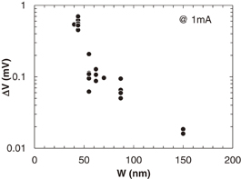
Fig. 4. Element size dependence of output voltage at an injection current of 1 mA. The annealing temperature was 400 °C.
Download figure:
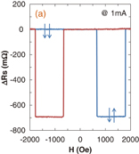
Standard image High-resolution imageThe nonlocal magnetoresistance hysteresis loop for the sample that showed the highest ΔV is shown in Fig. 5(a). A clear switching behavior in the nonlocal resistance between parallel (↑↑) and antiparallel (↑↓) spin configurations of the FM1 and FM2 wires is shown. The highest resistance change (output) of as large as 700 mΩ was observed for the sample with the junction of 40 × 55 nm2. The injection current dependence of the output for this sample is shown in Fig. 5(b). The output increased with the injection current, and the maximum output voltage was 1.2 mV at 2 mA. An injection current of more than 2 mA caused a break in the current lines. Since the current density was about 160 MA/cm2 for 2 mA and the length is around 10 µm, the Joule heating might cause the saturation tendency shown in Fig. 5 as well as electromigration.
Download figure:
Standard image High-resolution image
Fig. 5. (a) Typical nonlocal magnetoresistance hysteresis loop of a sample with element size of 40 × 55 nm2. (b) Injection current dependence of the output voltage for this sample.
Download figure:
Standard image High-resolution imageExperimental results for the NLSV samples are analyzed using the following equation of a one-dimensional model:17)
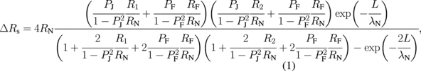
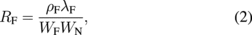

Here, PJ and PF are the interfacial and bulk polarizations of CMFS, RN and RF are the spin resistances of Cu and CFMS, λN and λF are the spin diffusion lengths of Cu and CFMS, L is the distance between the two CFMS wires [Wgap in Fig. 1(a)], WN and WF are the widths of the Cu and CFMS wires, tN is the thickness of the Cu wire, and R1 and R2 are the junction resistances of the FM1 and FM2 wires, respectively. λF is set to 2.1 nm from the value in the literature.11) The resistivities ρF and ρN are 80 and 3.3 µΩ·cm, respectively, from experimental results. The contribution of the interfacial spin scattering term is negligibly small compared with that of the bulk scattering term for an ohmic junction with an areal resistance of RA < 1 mΩ·µm2. The experimental data were fitted with the fitting parameters λN and PF. The fitting results for the experimental data are shown in Figs. 6(a) and 6(b). λN is fixed at 200 nm for Fig. 6(a), and PF is fixed at 0.7 for Fig. 6(b). Solid lines are theoretical lines. The best fitting result is obtained for PF = 0.7 and λN = 200 nm. This result indicates that the spin diffusion length is not degraded even for a junction size of 40 nm.

Download figure:
Standard image High-resolution image
Fig. 6. Results of fitting the one-dimensional model to the experimental data. (a) Bulk polarization (PF) dependence with fixed spin diffusion length of Cu: λN = 200 nm. (b) λN dependence with fixed PF = 0.7.
Download figure:
Standard image High-resolution imageAn increase in the output is estimated for NLSVs with further reduced element size using the one-dimensional model. As indicated in Fig. 7(a), the width of the FM1 wire was set to 30 nm. The current density was assumed to be 200 MA/cm2. Since heat dissipation around the magnetic junction area is high for the actual read head design, this current density may cause little heating problem, as shown in Fig. 5(b). Actually, the current density of 200 MA/cm2 was reported to be acceptable to a read head for an areal density of about 5 Tbit/in.2.18) Figure 7(b) shows the estimated output and injection current as a function of the FM2 wire width (W). The output voltage increases to 8 mV when the element size is reduced to 10 nm. Although we used a large value of λN for W = 10 to 50 nm, the output clearly increases even at W = 10 nm. This indicates that junction area reduction is the main cause of the output increase. The reduction in the junction area improves the spin resistance matching. The output voltage of 10 mV is close to that of conventional current-perpendicular-to-plane giant magnetoresistance (CPP-GMR) sensors (10 to 20 mV). Further increases in output are also expected by using low-RA junctions (0.1 Ω·µm2 or less) to improve the spin resistance matching,19) by dual-pin current injection,20,21) and by improving the spin polarization of Heusler alloys. The dual-pin structure of NLSVs does not cause any increase in read gap length owing to a recessed pinned structure, in contrast to CPP-GMR sensors. Because of the low RA and high output, NLSVs have good scalability for not only read gap length but also sensing track width, making them promising candidates for future high-density hard disk drive readers.
Download figure:
Standard image High-resolution image
Fig. 7. Estimated output voltage in the case of reduced element size. (a) Schematic illustration of the estimation model (WF1 = 30 nm, WF2 = WN = Wgap = W). (b) Estimates of output voltage and injection current with the following parameter settings: λF = 2.1 nm; λN = 200 nm; PF = 0.8; ρF = 80 µΩ·cm; ρN = 4.5 µΩ·cm; tN = 8 nm; current density = 200 MA/cm2. The red line indicates output voltage and the blue line indicates injection current.
Download figure:
Standard image High-resolution image
Acknowledgments
The authors acknowledge Dr. S. Kasai, Dr. Y. Sakuraba, and Dr. Y. K. Takahashi for numerous helpful discussions. This study was partially supported by the NEDO Strategic Innovation Program for Energy Conservation Technologies.