

Abstract
We fabricate GaAs-based triangular barrier photodiodes (TBPs), in which type-II GaSb quantum dots (QDs) are embedded in the vertex part of their triangular barriers. Their current–voltage characteristics and photo-responses are studied at low temperatures to show that GaSb QDs enhance the number and lifetime of photo-generated holes that are trapped by QDs in the barrier, resulting in the increase in the electron current around positively charged QDs. An extremely high responsivity of 109 A/W is achieved.
Export citation and abstract BibTeX RIS
Triangular barrier (TB) diodes are normally formed by inserting a thin layer of acceptors into an undoped semiconductor, sandwiched by a pair of n-type electrodes.1) As shown in Fig. 1, holes in the system are depleted, making the acceptor layer negatively charged. Thus, the formed TB repels electrons and attracts holes. TB diodes operate as photodetectors of high responsivities because photoholes are trapped in the acceptor layer and lower the barrier to enhance the current. This detection scheme is slow but yields a high photoconductive gain of several thousands, enabling the detection of weak light of the nanowatt level.2) This type of detectors may be important in various applications, such as astronomical observations, where the responsivity is more important than the speed.
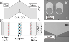
Fig. 1. (a) Band profile and (b) the structure of a GaAs TB diode with type-II GaSb QDs. The locations of negatively charged acceptors and positively charged donors at the edge of the electrode region are shown in (b). (c) and (d) show the top views of type-A and type-B diodes, respectively.
Download figure:
Standard image High-resolution imageTo improve the performance of TB photodiodes (TBPs), we have recently fabricated a TBP, where InGaAs quantum rods (QRs) are embedded within the TB to force electrons to flow through QRs.5) The responsivity of such QR-TBPs reaches 105 A/W because photoholes are trapped by rods and lower the barrier, thus enhancing the current through QRs. In this work, we explore another way to improve the performances of TBPs by employing a structure, where a sheet of type-II GaSb quantum dots (QDs) is inserted in the vertex of a GaAs TB, so that photoholes are trapped by QDs and lower the local barrier height around charged dots. We show that the photo-responses of such QD-TBPs are governed by the long lifetime nature of holes in QDs and their performances are compared to those of other QD-based photodetectors.
Yusa and Sakaki6) and Shields et al.7) studied QD-based photodetectors, where InAs QDs were buried between the channel and gate of an AlGaAs/GaAs field effect transistor (FET), so that photo-holes trapped by QDs shifted the threshold voltage. FETs with embedded QDs, biased below their threshold voltages and illuminated using weak light, showed a step-like increase in the conductance.7) This increase can be attributed to the trapping of a single photohole, which charges a QD near the constricted channel and opens a path for electrons. Although this scheme is attractive, the sensitivity is low because a photohole is not always trapped by a QD that opens a critical path of the current.
This weakness of FET-based QD photodetectors may be eliminated by placing QDs near the apex of TB or resonant tunneling (RT) diodes because photoholes may be driven to the barrier region and trapped by QDs. This may lower the local barrier and open current paths, as illustrated in Fig. 2. While Shields et al. studied an RT-QD structure with InAs QDs,8–10) we employed type-II GaSb QDs embedded in a GaAs TB11–15), which worked as deep trap sites for holes and low barriers for electrons. At cryogenic temperatures, when the electron transport becomes ballistic, a current path opens around a charged dot in a manner similar to opening the channel in a quantum point contact.16,17)
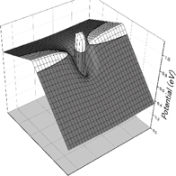
Fig. 2. Computed potential profile of the conduction band edge for a biased TB diode with a positively charged GaSb QD. A current path opens around the QD, a situation similar to a quantum point contact.
Download figure:
Standard image High-resolution imageWhen GaSb QDs in TBPs capture two or more holes, the barrier lowers in proportion to the number of trapped holes. If the electron flow over the barrier is dominated by thermal emission and/or voltage-dependent tunneling, this barrier lowering around charged dots makes the current grow exponentially with time. If the density of charged QDs is so high that their average spacing is less than the dot-to-electrode distance, the barrier lowering is determined by an ensemble of accumulated holes, as in the case of normal TBPs without QDs. Next, we describe the fabrication and detector characteristics of QD-TBPs.
To fabricate QD-TBPs, wafers were grown using molecular beam epitaxy on n-doped GaAs (311)A substrates with donor density ND of 1.5 × 1018 cm−3. As shown in Fig. 1, first, we grew 300-nm-thick n-type GaAs with ND of 1.0 × 1018 cm−3 to form a bottom electrode. Then we grew the bottom part of a TB by depositing 150-nm-thick undoped GaAs. Then the apex layer was formed by depositing 3.1-nm-thick GaAs with acceptor density NA of 1.0 × 1018 cm−3, 1-nm-thick undoped GaAs spacer, GaSb QD layer with sheet density σQD of 3.8 × 1010 cm−2, 15-nm-thick undoped cap layer, and 3.1-nm-thick acceptor-doped GaAs with density NA of 1.0 × 1018 cm−3. On top of this, we grew another 150-nm-thick undoped GaAs and a top electrode layer that consisted of 150-nm-thick GaAs with ND of 1.0 × 10¹⁸ and 50-nm-thick GaAs with ND of 3.0 × 1018 cm−3. Self-organized GaSb quantum dots were formed by depositing 2 monolayers (MLs) of GaSb.13–15) Si atoms were used as donors and acceptors by controlling their amphoteric nature, which depends on the growth condition. Using the wafer, two types of diodes (type A and B) were fabricated using mesa etching and ohmic contact formation. As shown in Fig. 1, the diode area and the photosensitive area of the type-A diode are  mm2 and
  mm2, respectively. Those of the type-B diode are
  µm2 and
  µm2.
µm2.
As the sheet density σA of acceptors is approximately 6.2 × 1011 cm−2, this negatively charged sheet should induce a TB of with a height of approximately 700 meV. From the temperature dependence of the current, the barrier height is determined to be ∼630 meV. Type-II GaSb QDs in GaAs serve as a deep potential well for holes, having the ground hole level of approximately 400 meV above the valence band edge.11–15) There are no holes in QDs in the dark, since the hole level is considerably below the Fermi level. This separation of electrons and holes reduces the recombination rate and prolongs the lifetime of holes.12)
First, the current–voltage (I–V) characteristics of the type-A diode were measured at a temperature of 77 K, as shown by curves from (1) to (5) in Fig. 3. Curve (1) is the I–V characteristics in the dark. It shows that the current in the low-bias region is very low. This suggests that the leakage current along the unpassivated side surface of the device is negligibly low, possibly because of the Fermi-level pinning effect of the GaAs surfaces. The current increases exponentially as bias voltage V is increased, indicating that the barrier lowering takes place in proportion to the bias voltage. This is consistent with the expectation that the TB is lowered by about half of bias voltage V. Once the current density reaches 1 mA/cm−2, the current does not increase exponentially further and tends to saturate. This suggests that the series resistance and/or the space charge effect become important. The I–V characteristics slightly depend on the polarity of bias, suggesting slight asymmetry of the band profile. This may result from the deviation of the dopant profile from the intended profile caused by the segregation of dopants and/or from the asymmetry of the contact resistance of the electrodes.
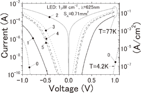
Fig. 3. I–V characteristics of the TB diodes with type-II GaSb QDs. Curves from (1) to (5) were measured using the type-A diode at a temperature of 77 K under the following conditions: (1) in the dark; (2) under an LED illumination; and (3), (4), and (5) were measured for 1, 10, and 30 min after turning off the LED. Curve (0) is the I–V characteristics of the type-B diode measured in the dark at 4.2 K. The current density axis located at the right side is valid only for curves from (1) to (5) and not valid for curve (0).
Download figure:
Standard image High-resolution imageWhen the device is exposed to LED light with a wavelength of 625 nm and a power of 3.5 nW, the current exhibits a dramatic increase in the region of low bias as shown using curve (2). This indicates that the TB is nearly eliminated because of the accumulation of photoholes. When the LED was turned off, the current decreased rapidly in the beginning and reached a semistable state, indicating that some holes were trapped by QDs for a long time. Curves (3), (4), and (5) are the I–V characteristics measured for 1, 10, and 30 min after turning off the LED. We conducted similar measurements using monochromatic light and confirmed that QD-TBPs work if the photon energy exceeds the bandgap of GaAs. LED light is mostly absorbed within the thickness of less than a micron from the surface, since the absorption constant is 4 × 104 cm−1. Holes are accumulated in the TB region and trapped by QDs.
Curves from (3) to (5) are similar to curve (1) measured in the dark except for the fact that curves from (3) to (5) are parallel-shifted towards lower biases by about 200–300 mV. This suggests that the barrier is persistently lowered by about 100–150 meV because of the illumination. From this shift, the density of holes trapped by QDs is calculated to be (1–1.5) × 1011 cm−2. As the density of GaSb QDs is 3.8 × 1010 cm−2, the number of holes trapped in each QD is calculated to be about 2.5–4. The electronic structure of GaSb QDs has been studied theoretically and using photoluminescence as well as capacitance–voltage measurements.9–12) It has been found that a GaSb QD accommodate as many as 14 holes, since the dot has a deep ground state and several excited states because of its shape and a deep potential well for holes.11) This makes the lifetime of trapped holes extremely long as will be discussed later.
We also studied the I–V characteristics of the type-B diode at a temperature of 4.2 K without LED illumination. The result is shown as curve (0) in Fig. 3. The exponential increase in current was found at 4.2 K at bias voltages higher those at 77 K, indicating that in this case, the transport of electrons is dominated by the voltage-dependent tunneling process.
We also investigated the temporal evolution of the photocurrent, as shown in Figs. 4 and 5. The left curve in Fig. 4, measured at a bias voltage of −0.9 V, shows that when the LED is turned on, the current increases exponentially for approximately 1500 s. This indicates that the barrier height of the TB is lowered in proportion to the duration of the illumination. Therefore, photoholes are trapped by QDs at a constant rate. After this exponential increase, the current tends to become saturated at a current of about 10−7 A or a current density of about 10−1 A/cm2, suggesting that the number of trapped holes does not increase further and reaches a steady state value. This temporal change of density σh of holes can be modeled and approximately expressed using the equation σh = gτ[1 − exp(−t/τ)], where g is the generation or incident rate of holes in QDs and τ is the characteristic time of the hole escape from QDs. τ of holes in excited states is approximately 1000 s, whereas τ of a ground state hole is significantly longer as discussed later. First, σh grows as gt. Finally, it becomes saturated at value gτ.

Fig. 4. Temporal evolution of the photocurrent at a temperature of 4.2 K measured using the type-B diode under the LED illumination at two different bias voltages.
Download figure:
Standard image High-resolution image
Fig. 5. Temporal evolution of the photocurrent at a temperature of 4.2 K measured using the type-B diode under constant LED illumination.
Download figure:
Standard image High-resolution image
The I–t curve at the right side of Fig. 4, measured at a bias voltage of −0.8 V, shows that initially the current is below the detection limit of a current meter (around 10−11 A). However, it starts to increase exponentially once the illumination time exceeds 1000 s. The subsequent temporal evolution of the current is similar to the left curve, measured at a bias voltage of −0.9 V, except for the fact that these two curves are shifted horizontally by approximately 1000 s. This indicates that the 1000-s-long illumination supplies a sufficient number of holes in the diode that charge QDs, so that the barrier height is lowered by approximately 50 meV to compensate a bias voltage difference of 100 mV. This lowering of the barrier height by 50 meV shows that density σh of holes accumulated for the period of 1000 s is approximately 5 × 1010 cm−2, or equivalently, hole generation rate g is approximately 5 × 107 cm−2 s−1. As the incident LED light intensity is 50 pW/cm2, its photon flux is 1.6 × 108 cm−2 s−1. This indicates that approximately 30% of photoholes are trapped by QDs.
When the LED power is increased by a factor of 10, the barrier lowering process or the exponential increase in the current is accelerated by 10 times, bringing the system to the photocurrent saturation regime for 1/10 of the period. The magnitude of the saturation current also increases as more holes are accumulated in QDs. However, once the average number of holes in each dot becomes approximately 10, the escape process of holes becomes faster and prevents the further increase in the current.
Now we examine the region of photocurrent saturation in Fig. 4. The presence of this region indicates that the process of the hole escape from QDs is balanced with the supply process of holes generated by photons, and therefore density σh of holes trapped by QDs reaches its steady-state value gτ of around (5–7.5) × 1010 cm−2. This hole escape process can be further evaluated by analyzing the last part of the I–t curves in Fig. 4, where the current decays with an effective time constant of about 1000–1500 s after turning off the LED. This long escape time originates from the uniqueness of GaSb QDs where holes are accommodated in deep energy levels. The process of the escape from QDs can be accelerated if a voltage of 1.8 V or higher is applied to the diode, which permits the resetting of the device.
The information extracted from Fig. 4 indicates that in the current saturation region, the effective barrier height for electrons is reduced to approximately 125 meV. This lowering of the barrier can also be achieved by applying bias voltage VB of −1 V. The current starts to deviate from the exponential relation and tends to become saturated, as shown in Fig. 3. As shown in in Fig. 4, the temporal change in the saturation current for VB = −0.8 V is similar to that for −0.9 V, indicating that the barrier height is dominated by accumulated holes rather than by the bias voltage.
Next, we evaluate the responsivity of QD-TB detectors from Fig. 4. Since photocurrent ΔIph in the region of saturation is approximately 0.3 µA and power P of incoming light is 1.5 × 10⁻¹⁶ W (= 50 pW/cm2 × 289 × 10−8 cm2), responsivity  is ∼2 × 10⁹ A/W. This value is almost 106 times higher than that of a conventional TBP1–4) and 104 times higher than that of a quantum rod TBP.5) Here, the responsivity is defined in the region of the saturation current, which is reached after long illumination.
We have examined the temporal evolution of the photocurrent focusing on the exponential increase and the current saturation region so far. Now we study an earlier stage of the I–t curve before the exponential increase begins. As shown in Fig. 5, the current at a temperature of 4.2 K for bias voltage Vb of 1 V is dominated by the dark current. When the illumination begins, the current increases linearly for approximately 50 s. Then it increases exponentially. This linear increase occurs only for a short time under restricted conditions; for example, the full resetting of the diode to its initial dark state is necessary. Holes trapped in QDs can be removed by applying a bias voltage of 1.8 V or higher because in this case the barrier effect for electrons vanishes, allowing the ample supply of electrons to the region of QDs. These electrons recombine with holes and erase all the holes, allowing the full resetting of the device. This linear increase suggests that each hole generated by incoming photons is trapped by an individual QD and opens a current path around the dot in such a way that the increase in the photocurrent is linearly proportional to the number of incident photons and to that of charged QDs.
In this experiment, the light intensity is 0.3 nW/cm2, which is 6 times higher than that for Fig. 4. This indicates that the generation or supply rate g of holes is approximately 3 × 108 cm−2 s−1. As the density of holes accumulated for the first 10 s is estimated to be 3 × 109 cm−2, this suggests that only 1/10 of QDs is positively charged at this stage. As the average spacing of such charged dots is approximately 170 nm, each charged dot is likely to work almost independently and lowers the local potential around the dot to enhance the current through a new path near the dot. As the illumination continues, more QDs become positively charged, and eventually the average spacing of charged dots becomes less than the distance between the QD layer and the electrode. Then the barrier lowering is controlled by an ensemble of charged dots, leading to the exponential growth of the current as in the case of a normal TBP.
Figure 5 shows that the current increase for the illumination for the first 20 s is approximately 1 nA. Since the number of QDs charged during this period is estimated to be approximately 15000 (= SB × 5 × 109 cm−2), the increase in the current for each charged QD is calculated to be approximately 70 fA. Though the presence of this linear response region suggests a potential of operating the device in the photon-counting mode, the sensitivity achieved so far is still too low to be practical. Therefore, the device structure needs to be improved by suppressing the dark current and enhancing the conductance increase induced by charging a one dot. For these objectives, the device area needs to be reduced to several µm2. In addition, the density of QDs should be lowered to reduce the number of QDs in each diode to one or a few, so that single or a few holes generated by photons are trapped by these QDs in order to enhance the local barrier lowering. Moreover, InGaSb QDs are desirable to be used instead of GaSb dots, which reduce the repulsive action of GaSb QDs to electrons and enhance the light-induced increase in the current flowing around a charged QD.
Finally, we briefly discuss noise aspects of TBPs. First, normally biased QD-TBPs and Schottky diodes behave similarly in the dark as electrons carry the current. Therefore, the dark current is subject to thermal noise, shot noise, and 1/f-type noise components, which depend on the bandwidth and the temperature. However, under illumination, the two devices behave quite differently, since photoholes are swept away in the Schottky diodes, whereas they are kept for 1000 s or longer in the QD-TBPs lowering the barrier height and increasing the current. Because of this long trapping time, the QD-TBPs operate with a narrow effective bandwidth at low temperatures, suggesting that thermal noise is negligible. On the other hand, fluctuations in the number of trapped holes may generate 1/f-type noise as they affect the barrier height and the current. Moreover, this leads to a random telegraph noise in the small-current regime. Noise issues in QD-TBPs are important and need to be further studied in the future.
In summary, the introduction of GaSb QDs into TBPs greatly alters the photo-responses of TBPs and allows an increase in their responsivity of up to 109 A/W. This originates from the trapping of holes in deep energy levels of GaSb QDs, that increase the hole lifetime to 1000 s or longer.
Acknowledgment
We thank the Grant-in-Aid for Basic Scientific Research of MEXT and support by Canon Foundation.