

Abstract
We demonstrated low-resistivity GaInN-based tunnel junctions using graded GaInN layers. A systematic investigation of the samples grown by metalorganic vapor phase epitaxy revealed that a tunnel junction consisting of a 4 nm both-sides graded GaInN layer (Mg: 1 × 1020 cm−3) and a 2 nm GaN layer (Si: 7 × 1020 cm−3) showed the lowest specific series resistance of 2.3 × 10⁻⁴ Ω cm2 at 3 kA/cm2 in our experiment. The InN mole fraction in the 4 nm both-sides graded GaInN layer was changed from 0 through 0.4 to 0. The obtained resistance is comparable to those of standard p-contacts with Ni/Au and MBE-grown tunnel junctions.
Export citation and abstract BibTeX RIS
The first GaInN-based tunnel junction for current injection from n-layers to p-layers was demonstrated in 2001.1) Because the tunnel junctions made of other III–V semiconductors have been adopted in various devices,2–4) such a GaInN-based tunnel junction is also expected to be utilized to improve device performance in not just tandem solar cells5) and cascaded LEDs,6–12) but also in micro-LEDs,13,14) their arrays,15) lasers,16,17) and vertical cavity surface emitting lasers (VCSELs).6,18) At that time, however, the voltage drop at the GaInN tunnel junction was high, about 0.6 V at 50 A/cm2, and further reduction in tunnel junction resistance was demanded.
In 2010, a new concept to leverage polarization charges at the GaInN/GaN interfaces was proposed towards realizing low-resistivity GaInN-based tunnel junctions.19) Thus, the GaInN layer has been used in the tunnel junctions because of not only a narrower band gap20) with a lower ionized energy of a Mg acceptor21) but also the polarization doping. Since then, the GaInN-based tunnel junctions have shown marked improvements in their reverse-biased characteristics. In particular, a GaInN tunnel junction grown by MBE showed a very low specific series resistance of 1.2 × 10⁻⁴ Ω cm2.22) On the other hand, a GaInN tunnel junction grown by metalorganic vapor phase epitaxy (MOVPE) showed a resistance of 4.0 × 10⁻⁴ Ω cm2 by using a very high InN mole fraction of 0.4 and lateral Mg activation.23–25) However, a large voltage drop at the GaInN tunnel junction of about 1 V was still observed under operation with a high current density of ∼3 kA/cm2.
In this study, we paid attention to not only a tunneling probability component in the GaInN layer but also an energy spike component at the GaInN/GaN interfaces in terms of the resistance of the GaInN tunnel junction. The GaInN layer with the high InN mole fraction leads to a high tunneling probability owing to the small band gap, but at the same time generates large energy spikes at the GaInN/GaN interfaces, which result in a high resistance. Such energy spikes are notorious as a cause of the large resistance in semiconductor-based devices, such as distributed Bragg reflectors. In order to eliminate such energy spikes, graded layers were proposed and often used.26,27) Actually, the effect of the graded AlGaN layers in a GaN/AlN tunnel junction was theoretically investigated by Schubert.28) Here, we experimentally investigated the impact of the graded GaInN layers on the resistance of the GaInN tunnel junctions. Various InN mole fraction profiles in the graded GaInN tunnel junctions were also determined. As a result, we demonstrated a graded GaInN tunnel junction with a very low resistivity, the specific series resistance of which was 2.3 × 10⁻⁴ Ω cm2 at 3 kA/cm2.
All the samples were grown by MOVPE on c-plane sapphire substrates using low-temperature-deposited buffer layers.29) As shown in Fig. 1, a sample structure consisted of a standard blue LED structure, a GaInN-based tunnel junction, a 400 nm top n-GaN layer, and a 10 nm n+-GaN contact layer. We prepared four samples containing different GaInN layers in the tunnel junctions. Figure 2 shows the designed InN mole fraction profiles in the GaInN layers. The first sample shown in Fig. 2(a) contained a 2 nm2 Ga0.6In0.4N layer, which was the same layer that we previously optimized.24) The other three samples contained graded GaInN layers. The second sample shown in Fig. 2(b) had a 4 nm p-side graded GaInN layer in which the InN mole fraction was increased from 0 at the p-side (left) to 0.4 at the n-side (right). The third sample included the opposite n-side graded GaInN layer in which the InN mole fraction was decreased from 0.4 at the p-side to 0 at the n-side, as shown in Fig. 2(c). Finally, as shown in Fig. 2(d), the fourth sample contained a 4 nm both-sides graded GaInN layer in which the InN mole fraction was changed from 0 to 0.4 in a 2 nm p-side GaInN layer and from 0.4 to 0 in a 2 nm n-side GaInN layer. In other words, the InN mole fraction profile of the both-sides graded GaInN layer was "Λ"-shaped. Here, the InN mole fractions were controlled by changing the TMIn flow rate during the graded GaInN layer growth while the growth temperature and TMGa flow rate remained constant. Note that the total amount of In in the tunnel junction was designed to be the same among all the samples. All the GaInN layers in the tunnel junctions were doped with Mg of 1 × 1020 cm−3. Then, 2 nm heavily Si-doped (7 × 1020 cm−3) GaN layers were grown on the GaInN layers to complete the tunnel junction structures.

Fig. 1. Sample structure consisting of a standard blue LED structure, a GaInN-based tunnel junction, a 400-nm top n-GaN layer, and a 10-nm n+-GaN contact layer.
Download figure:
Standard image High-resolution image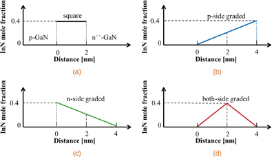
Fig. 2. Designed InN mole fraction profiles in the GaInN tunnel junctions: (a) a 2 nm2 Ga0.6In0.4N, (b) a 4 nm p-side graded GaInN, (c) a 4 nm n-side graded GaInN, and (d) a 4 nm both-sides graded GaInN.
Download figure:
Standard image High-resolution imageA lateral Mg activation previously developed for the LEDs with the tunnel junctions was performed for all the samples.25) After forming device mesas of 35 µm diameter, the wafers were thermally annealed under oxygen ambient at 725 °C for 30 min. Metal layers, Ti (30 nm)/Al (100 nm)/Ti (20 nm)/Au (150 nm), for the top and bottom n-contacts were simultaneously formed. Since the small mesas were formed, we were able to measure the current density–voltage (j–V) and current density–light output power (j–L) characteristics of the LEDs with the tunnel junctions under a high current density of up to 5 kA/cm2. For comparison, we also prepared a small standard blue LED with a p-contact with Ni/Au.
Figure 3 shows calculated band diagrams around the tunnel junctions in the four samples. Commercial software (SiLENSe)30) was used for the calculation. Large energy spikes were clearly shown at the interfaces of the 2 nm2 GaInN layer in Fig. 3(a). The energy heights of the spikes were 0.9 eV at the conduction band and 0.4 eV at the valence band. On the other hand, no energy spikes were shown at the p-side interface in the p-side graded GaInN tunnel junction [Fig. 3(b)] and at the n-side interface in the n-side graded GaInN tunnel junction [Fig. 3(c)] owing to the graded layers. Interestingly, even with the very thin graded layers (2 nm) [Fig. 3(d)], a clear reduction in the number of energy spikes was also shown at both interfaces in the both-sides graded GaInN tunnel junction.28)

Fig. 3. Calculated band diagrams around the GaInN tunnel junctions: (a) a 2 nm2 Ga0.6In0.4N, (b) a 4 nm p-side graded GaInN, (c) a 4 nm n-side graded GaInN, and (d) a 4 nm both-sides graded GaInN.
Download figure:
Standard image High-resolution imageFigure 4 shows the j–V characteristics of the four LEDs with the square GaInN tunnel junctions or various graded GaInN tunnel junctions. The operating voltage of the LED with the square GaInN tunnel junction was 5.3 V at 3 kA/cm2. On the other hand, all of the LEDs with the graded GaInN tunnel junctions showed lower operating voltages of 4.6 V or lower at 3 kA/cm2. The differential specific series resistance of the device was also estimated to be 2.3 × 10⁻⁴ Ω cm2 at 3 kA/cm2, suggesting that the tunnel junction resistance should be lower than this value, which is comparable to the best value of MBE-grown nitride-based tunnel junctions.22) These lines of evidence suggest that the energy spikes at the heterointerfaces have a considerable impact on the tunnel junction resistances. Note that the LED with the both-sides graded tunnel junction showed the lowest voltage of 4.3 V at 3 kA/cm2, but the value was not so low as expected in consideration of the results obtained from the single-side (the p- or n-side) graded tunnel junctions. One of the possible reasons is that the actual 2 nm graded GaInN layer could be too thin to eliminate the energy spike sufficiently.

Fig. 4. j–V characteristics of the four LEDs with the GaInN tunnel junctions containing the 2 nm2 Ga0.6In0.4N, 4 nm p-side graded GaInN, 4 nm n-side graded GaInN, or 4 nm both-sides graded GaInN.
Download figure:
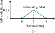
Standard image High-resolution imageThen, we attempted a larger graded layer thickness in the both-sides graded GaInN tunnel junction. We found that the sample surface deteriorated when we grew an 8 nm both-sides graded GaInN layer from 0 through 0.4 to 0 on the LED structure. It is difficult to obtain simultaneously a small band gap and thick graded layers with high InN mole fractions owing to the large lattice mismatch between GaInN and GaN. In other words, the choice of InN mole fraction in the graded GaInN tunnel junction affects two opposite aspects. One is the tunneling probability in which a "higher" InN mole fraction results in a lower resistance, and the other is the energy spike height in which a "lower" InN mole fraction results in a lower resistance. Therefore, an optimum InN mole fraction may exist in such a trade-off situation. We then prepared two additional LEDs with different both-sides graded GaInN tunnel junctions. As shown in Fig. 5, two different InN mole fraction profiles were obtained. The first one was a 6 nm both-sides graded GaInN layer with InN mole fractions from 0 through 0.35 to 0, as shown in Fig. 5(a). The second one was an 8 nm both-sides graded GaInN layer with InN mole fractions from 0 through 0.2 to 0, as shown in Fig. 5(b).
Download figure:
Standard image High-resolution image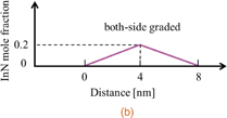
Fig. 5. Designed InN mole fraction profiles in the graded GaInN tunnel junctions: (a) a 6 nm both-sides graded Ga0.65In0.35N and (b) an 8 nm both-sides graded Ga0.8In0.2N.
Download figure:
Standard image High-resolution imageFigure 6 shows calculated band diagrams around the tunnel junctions in the two samples. No energy spikes were found at both interfaces in the two samples. Actually, as compared with the above-mentioned 4 nm both-sides graded GaInN tunnel junction in Fig. 3(d), the additional two samples containing the wider graded layer with the lower InN mole fraction showed smoother potential profiles but slightly larger depletion lengths. Figure 7 shows the j–V characteristics of the two additional both-sides graded GaInN tunnel junctions (6 and 8 nm) as well as the 4 nm both-sides graded GaInN tunnel junction. In this experiment, we found that the 4 nm graded GaInN layer with the 0.4 InN mole fraction still resulted in the lowest resistance.

Download figure:
Standard image High-resolution image
Fig. 6. Calculated band diagrams around the graded GaInN tunnel junctions: (a) a 6 nm both-sides graded Ga0.65In0.35N and (b) an 8 nm both-sides graded Ga0.8In0.2N.
Download figure:
Standard image High-resolution image
Fig. 7. j–V characteristics of the three LEDs with the tunnel junctions containing the 4 nm both-sides graded Ga0.6In0.4N, 6 nm both-sides graded Ga0.65In0.35N, or 8 nm both-sides graded Ga0.8In0.2N.
Download figure:
Standard image High-resolution imageEventually, we plotted the j–V–L characteristics of the LED with the 4 nm both-sides graded Ga0.6In0.4N tunnel junction showing the lowest resistance and the standard LED containing the p-contact with Ni/Au. Here, light output power was measured under the bottom emission configuration. As shown in Fig. 8, the operating voltage and light output power of the LED with the tunnel junction were comparable to those of the standard LED with p-contact.

Fig. 8. j–V–L characteristics of the LED with the 4 nm both-sides graded Ga0.6In0.4N tunnel junction and a standard LED with p-contact and Ni/Au.
Download figure:
Standard image High-resolution image
In this study, we investigated the impact of the graded GaInN layers on the resistance of the GaInN tunnel junctions grown by MOVPE. The experimental results revealed that the graded GaInN layers resulted in lower voltage drops at the tunnel junctions. Our lowest specific series resistance of the graded GaInN tunnel junction was 2.3 × 10⁻⁴ Ω cm2 at 3 kA/cm2 as obtained by using the 4 nm both-sides graded Ga0.6In0.4N layer. The value is now comparable to those of the standard p-contact with Ni/Au and the GaInN tunnel junction grown by MBE. Such a low-resistivity GaInN tunnel junction grown by MOVPE could open up great possibilities for high-performance nitride-based optoelectronic devices.
Acknowledgments
This work was supported by a Grant-in-Aid for Scientific Research (B) (No. 26286045), a Grant-in-Aid for Challenging Exploratory Research (No. 15K13959), and the Ministry of Education, Culture, Sports, Science and Technology (MEXT)-Supported Program for the Strategic Research Foundation at Private Universities, 2012–2016.