Abstract
Tungsten diselenide (WSe2) is an attractive transition metal dichalcogenide material, since its Fermi energy close to the mid gap makes it an excellent candidate for realizing p–n junction devices and complementary digital logic applications. Doping is one of the most important technologies for controlling the Fermi energy in semiconductors, including 2D materials. Here we present a simple, stable and controllable p-doping technique on a WSe2 monolayer, where a more p-typed WSe2 field effect transistor is realized by electron transfer from the WSe2 to the gold (Au) decorated on the WSe2 surfaces. Related changes in Raman spectroscopy are also reported. The p-doping caused by Au on WSe2 monolayers lowers the channel resistance by orders of magnitude. The effective hole mobility is ∼100 (cm2/Vs) and the near ideal subthreshold swing of ∼60 mV/decade and high on/off current ratio of >106 are observed. The Au deposited on the WSe2 also serves as a protection layer to prevent a reaction between the WSe2 and the environment, making the doping stable and promising for future scalable fabrication.
Export citation and abstract BibTeX RIS

Content from this work may be used under the terms of the Creative Commons Attribution 3.0 licence. Any further distribution of this work must maintain attribution to the author(s) and the title of the work, journal citation and DOI.
1. Introduction
Semiconducting two-dimensional (2D) graphene exhibits great potential for various applications, including electronics, optoelectronics, energy harvesting and sensors [1–3]. However, monolayer graphene does not have an energy bandgap, which makes it challenging to use as a field-effect transistor (FET) with a high on/off current ratio [4]. Although an energy gap up to 400 meV has been demonstrated by patterning graphene into narrow ribbons [5], significant mobility degradation and fabrication challenges limit its practical application in electronics. An energy gap can also be achieved by applying a perpendicular electric field to a bilayer graphene [6], but these gaps are smaller than 250 meV. Recently, the 2D material transition metal dichalcogenide (TMD), in which a sheet of metal atoms is sandwiched between two sheets of chalcogens by covalent bonds, has attracted great interest. The layer structure and unique electrical properties of semiconducting TMD monolayers make them suitable to serve as the channel in nanoelectronics. The monolayer TMD channels are resistant to short channel effects [7] and the lack of dangling bonds on their surfaces may result in a lower change scattering probability and fewer interface trap states [8].
One of the most frequently reported TMD materials for transistor applications is molybdenum disulphide (MoS2) because of its large intrinsic bandgap [9, 10]. MoS2 monolayers exhibit a direct bandgap of 1.8 eV [11, 12], and it has been reported that the monolayer MoS2 FETs exhibit a high electron mobility, an excellent on/off current ratio and a low subthreshold swing [9]. It is noted that most MoS2-based FETs exhibit n-type electrical characteristics since MoS2 is normally highly n-doped. Tungsten diselenide (WSe2) is another attractive TMD material since its Fermi energy is close to the mid gap [13], which makes it easier to realize p–n junction devices and complementary digital logic applications. Recent advances in the chemical vapour deposition (CVD) of MoS2 [14] and WSe2 [15] monolayers have allowed researchers to obtain large-area TMD samples, but to bring TMD research closer to practical applications, many important issues need to be resolved.
Doping is one of the critically important technologies in TMDs. Despite the fact that several doping techniques, including surface doping, edge doping, electrostatic doping and substitution doping, have been developed for MoS2 [16–21], it still remains a challenge to keep the doping stable and highly efficient. Moreover, the Fermi level engineering or doping in monolayer WSe2 is still relatively unexplored. Recently, Fang et al have reported transistors based on WSe2 using high-k materials as the gate dielectrics, where the chemically doped source/drain contacts exhibit low contact resistances. Selective treatment with potassium is able to form degenerately doped n+ contacts for electron injection while NO2 treatment forms p+ contacts [22–24]. Liu et al have demonstrated the n-type WSe2 FET by using indium as a contact metal [25]. Chuang et al have revealed that graphene can be a work-function-tunable electrode material for few-nanometre WSe2 FETs [26]. It is noted that the small molecules adsorbed on the 2D materials tend to desorb from the surfaces and the alkali metals are known to be sensitive to moisture and oxygen. In fact, most of the previous reports on chemical doping have shown that the electrical results change with time [27] and even with rinsing with water [28].
Here, we report a simple, stable and controllable p-doping technique on a WSe2 monolayer, where a more p-typed WSe2 FET is realized by electron transfer from the WSe2 to the Au decorated on the WSe2 surfaces. The p-doping effect from Au decoration is systematically evaluated by Raman spectroscopy, photoluminescence (PL), atomic force microscopy (AFM), ultraviolet photoemission spectroscopy (UPS) and electric double-layer transistor (EDLT) characterizations. The gold nanoparticle (AuNP) decoration on the WSe2 monolayer results in the channel resistance lowering by orders of magnitude and the p-type FET with an effective mobility of ∼100 (cm2/Vs), near the ideal subthreshold swing of ∼60 mV/decade and high on/off current ratio of >106. The Au deposited on WSe2 also serves as a protective layer to prevent reaction between the WSe2 and the environment, making the doping stable in ambient conditions.
2. Results and discussion
The direct growth of crystalline WSe2 monolayer film on a sapphire substrate by the vapour-phase reaction of WO3 and Se powders was performed in a hot-wall CVD system as described elsewhere [15]. Figure 1(a) displays the Raman spectra for a pristine WSe2 film, where the excitation light source is a continuous laser with a wavelength of 473 nm. Two characteristic peaks including E' (or E12g) at 249 cm−1 and A'1 (or A1g) at 250 cm−1 are identified [29–32]. The AFM image in figure S1 shows that the as-grown WSe2 film is mostly monolayer (thickness ∼0.72 nm). The film is up to few centimetres in lateral size and composed of WSe2 crystalline domains (a few microns in size) as described in reference [15]. The typical PL spectrum of an as-grown WSe2 monolayer in figure 1(b) shows one pronounced emission peak at 760 nm (1.63 eV), assigned as the A direct excitonic transition [11, 33]. Besides, the broad peak at 600 nm (2.06 eV) belonging to the B direct transition is not pronounced for as-grown WSe2 monolayer film, likely due to the fact that it is not the lowest energy transition [34, 35]. Another peak at a longer wavelength of 806 nm (1.54 eV), attributed to the indirect bandgap emission, is not pronounced for the monolayer WSe2. It is noted that the distinctly strong emission from a monolayer is in good agreement with the recent report [36–38].
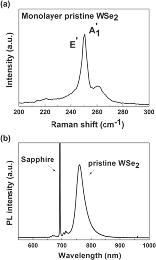
Figure 1. (a) The Raman spectrum for the CVD WSe2 monolayer. (b) The photoluminescence spectra for the CVD WSe2 monolayer.
Download figure:
Standard image High-resolution imageRaman spectroscopy is a nondestructive methodology used to reveal the doping effect in monolayer 2D materials. It has been established that the peak width and position of Raman A'1 band (∼402 cm−1) for monolayer MoS2 are sensitive to the Fermi energy change or carrier concentration [39]. Chakraborty et al have shown that n-doping results in a softening and intensity decrease of the A'1 phonon, while p-doping causes a blue shift and intensity increase of the A'1 phonon [17, 40]. It would be interesting to know whether the WSe2 layer is affected by the Au decoration or not. Figure 2(a) shows the Raman spectra for the pristine WSe2 monolayer film and those after thermal evaporation with Au its surfaces. The Au deposition was performed in a thermal evaporator, where the 10 s deposition corresponds to roughly 1 nm of Au in thickness interpolated from our established linear relation between Au thickness and deposition time for the system. Figure 2(b) shows that the 10 s Au deposited on WSe2 still remains as nanoparticles but the 20 s Au deposition appears film-like on WSe2 (supporting figure S2, available from stacks.iop.org/TDM/1/034001/mmedia). The characteristic peak for WSe2 at about 250 cm−1 is assigned to the E' and A'1 degenerated mode [41] (some other reports have termed this mode E' + A'1 [29–32]). With the decoration of Au on WSe2, the peak at 250 cm−1 displays a red shift, where the Raman intensity for each spectrum has been scaled for better comparison. We have also performed the Raman spatial mappings using confocal Raman spectroscopy, where the mappings were constructed by plotting the peak frequency on a false colour scale (laser spot focused to ∼1 μm diameter). Note that for the convenience of experiments, we used WSe2 triangular flakes for Raman mapping studies. Figure 2(c) shows the Raman E' + A'1 mappings for the selected WSe2 monolayer flake before and after deposition with 10 s of Au, where the mapping consistently shows the peak redshift after Au deposition. In addition to the change in Raman peak shift, figure 2(d) shows the PL spectra for the monolayer WSe2 flake with a strong emission at ∼760 nm corresponding to the A exciton, whereas the emission intensity of the same peak becomes much lower after Au deposition (10 s). Figure 2(e) shows the spatial PL mappings (excited by a 473 nm laser) for the WSe2 monolayer flake before and after it was deposited with Au, where the integrated peak area from 720 to 820 nm (linear baseline is applied in between 720 nm and 820 nm) is plotted as the false colour based on the colour index on the right. Hence, it can be concluded that Au deposited on WSe2 imposes a strong interaction to WSe2, which changes the optical properties of WSe2.
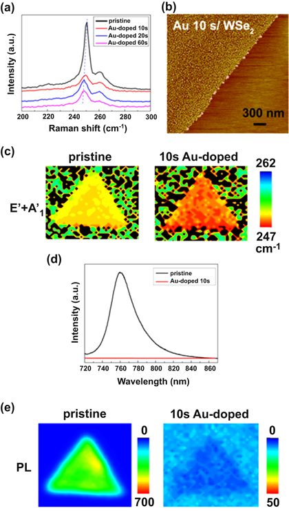
Figure 2. (a) Raman spectra evolution of the WSe2 monolayers with various Au deposition times in ambient conditions. The wavelength of the Raman laser is 473 nm, the spot size is ∼1 μm, and the power is ∼1 mW. (b) The AFM for the 10 s Au deposited on the WSe2 (rate = 1 Å s−1). (c) Raman mappings of the pristine and Au-decorated WSe2 constructed using E' + A'1 frequencies. (d) The photoluminescence spectra and (e) mappings for the pristine and 10 s Au-decorated WSe2 monolayer flakes.
Download figure:
Standard image High-resolution imageTo understand whether the Au deposition results in doping, we measured the electrical properties of the EDLTs based on the WSe2 monolayer films on sapphire substrates. EDLT is known as a method to determine electrical characteristics at a high carrier concentration, which is not easily accessed by solid insulator gating. The detailed EDLT fabrication processes have been reported elsewhere [15, 42]. Figure 3(a) schematically illustrates the structure of the EDLT device, where the 2 nm Ni and 70 nm Au were deposited by thermal evaporation on the source and drain contact areas with a hard mask. The ion gels, a mixture of a triblock copolymer, poly(styrene-block-methyl methacrylate-block-styrene) and an ionic liquid, 1-ethyl-3-methylimidazolium bis(trifluoromethylsulfonyl) imide, are used as the top gate dielectrics as described in our previous publication [43]. The transistor channel was then covered with a thin Pt foil as the top-gate electrode. A separate thin Au wire was inserted into the gel as the reference electrode. Figure 3(b) shows a photograph of the EDLT device top view, where the channel width and length are 70 and 1000 μm, respectively. The room-temperature transfer characteristics of a monolayer WSe2 EDLT under different VR values are shown on a linear scale in figure 3(c) and on a logarithmic scale in figure 3(d). Note that the VR is the measured voltage between the electrolytes and WSe2, the voltage for the electric double layer on WSe2 surfaces, and it is normally used as the effective gate voltage in EDLTs [43]. The pristine WSe2 EDLTs show typical ambipolar behaviours which are consistent with our previous reports [15]. Figure 3(c) also presents the p- and n-transfer curves (drain current ID vs VR) of Au-decorated WSe2 monolayer EDLT at the applied drain voltage VD = −0.1 and 0.1 V, respectively. The fact that the ID (Au-decorated) is higher than ID (pristine) in the p-channel but lower in the n-channel indicates that Au decoration imposes p-doping to WSe2. That the threshold voltage of the p-channel changes from −1.21 V for pristine WSe2 to −0.95 V for Au-decorated (n-channel from 0.93 to 1.78 V) also suggests a p-doing effect by the Au decoration. And that the hole threshold voltage decreases after Au-doping indicates that the Au-doped WSe2 can operate at a low gate voltage. Moreover, the field-effect mobility was calculated by the standard formula for the linear region, μ = (L/WCiVD)—(ΔID/ΔVR), where μ is the field-effect mobility, W is the channel width, VD is the drain voltage, Ci is the measured specific capacitance of the ion gel, L is the channel length, and ID is the drain current. The inset in each graph plots the reference voltage dependence of carrier mobilities. The highest carrier mobility of the hole transport increases from 55 to 96.6 cm2 Vs−1 after Au-doping, which is around twice as large as the pristine WSe2 EDLT. On the other hand, the electron mobility decreases from 8.15 to 3.67 cm2 Vs−1. Figure 3(d) shows the drain current from a linear to a log scale, and the on/off current ratios are ∼105 and 104 for p- and n-channels in pristine WSe2 EDLTs. The on/off ratio for the EDLT after Au-doping increases by one order of magnitude for p- and n-channels. The subthreshold swing was estimated to be 68 mV/decade after 10 s Au-deposition, which is close to the theoretical limit of 60 mV/decade. As shown in figure 3(e), ideal Ohmic-like contacts and a reasonable saturation behaviour were observed, resulting in sufficient current amplification. The electrical characteristics for the EDLTs fabricated with the WSe2 films with various Au deposition times (0, 10, 20 and 60 s) are summarized in table 1. We notice that although a longer deposition time (say 60 s) can p-dope the WSe2 and totally suppress the n-channel conduction, the overloaded Au on WSe2 likely introduces many scattering sites which also largely degrade the p-channel mobility.

Figure 3. (a) Schematic diagram of the WSe2 EDLT constructed with an ion gel on a sapphire substrate. The source/drain electrodes were composed of Ni/Au. (b) Optical micrographs of the top view for the WSe2 EDLT device which were taken before and after the ion gel/top gate deposition. (c) Transfer characteristics of the WSe2 EDLT under different treatments on a linear scale. VD is the drain voltage, and VR is the measured voltage between the electrolytes and WSe2. The red and blue lines correspond to the transfer curve for the WSe2 before and after the doping, respectively. The left photo shows the p-channel transfer curve, right is the n-channel transfer curve. The inset shows the carrier mobility values measured at various reference voltages. The drain voltage level was maintained at ±0.1 V, which was in the linear regime. (d) The transfer curves of the pristine and p-doped WSe2 plotted in a log scale. (e) Output characteristics of the pristine and p-doped WSe2.
Download figure:
Standard image High-resolution imageTable 1. EDLT characteristics for the WSe2 monolayers deposited with 0 s, 10 s, 20 s and 60 s of Au respectively.
| Hole | Electron | |||||||
|---|---|---|---|---|---|---|---|---|
| Device | Vth(V) | m(cm2 Vs−1) | S(mV dec−1) | C(μF cm−2) | Vth(V) | m(cm2 Vs−1) | S(mV dec−1) | C(μF cm−2) |
| pristine | 1.21 ± 0.06 | 55 | 100 | ∼5.1 | 0.93 ± 0.16 | 8.15 | 88 | ∼3.8 |
| 10 sec-doped | 0.95 ± 0.07 | 96.6 | 68 | ∼4.9 | 1.78 | 3.67 | 126 | ∼4.2 |
| 20 sec-doped | 0.96 ± 0.03 | 90.5 | 108 | ∼7.8 | 1.46 | 0.70 | 93 | ∼5.3 |
| 60 sec-doped | 1.00 ± 0.10 | 9.00 | 248 | ∼7.4 | — | — | — | — |
To further strengthen the p-doping argument, we used UPS to reveal the Fermi-level change after Au-doping. The as-grown monolayer WSe2 films on sapphire were transferred by PMMA-assisted wet chemical process on 1.5 × 1.5 cm silicon substrates for UPS measurements. In figure 4(a), the photoemission spectra were excited by helium I with a photon energy of 21.2 eV and corrected to zero point as the Fermi-level. From the tangent line of the on-set part, we obtain the difference of the valence-band-maximum and Fermi-level (VBM-EF) with values of 1.8 eV and 1.37 eV (w.r.t. EF) for the pristine and Au-doped WSe2 films respectively. The Fermi energy of WSe2 was lowered by about 0.43 eV after Au-doping, corroborating that Au decoration p-dopes the WSe2. In the figure 4(b), the photoemission spectrum was injected by the helium II with a photon energy of 40.8 eV and corrected to zero point as the Fermi-level. In the off-set region, we acquire the cut-off values 37.19 eV and 36.76 eV w.r.t. EF to pristine WSe2 and Au-doped WSe2 respectively. These cut-off values are described as the largest extractable electron states in the measured samples. Moreover, the differences of the injected photon energy and the cut-off value are defined as the work function. Thus, we could obtain a work function of 3.61 eV of pristine WSe2 and 4.04 eV of Au-doped WSe2, respectively. The work function moves away from the vacuum level after Au-doping. Combining these results, the band structure of WSe2 could be derived as shown in figure 4(c). The Fermi energy is obviously decreased about 0.43 eV after Au decoration. In addition, the distance of vacuum level to VBM was kept the same as 5.41 eV after Au decorated on WSe2, which showed that there is no chemical reaction between Au and WSe2 during the Au evaporation process.

Figure 4. Characterization of pristine and Au-doped (10 s) WSe2 monolayer using UPS. (a) The tangent line of the on-set part; (b) the off-set part. (c) Schematic illustration for the band structure of p-doping WSe2.
Download figure:
Standard image High-resolution image
3. Conclusions
In summary, we have revealed that Au decoration results in successful p-doping of the monolayer WSe2. Electrical characterization using EDLTs and Fermi energy measurements by UPS confirm the p-doping behaviours. The p-doping in WSe2 results in the redshift of the major Raman peak at ∼250 cm−1 although this mode is a degenerate mode of Raman E' + A'1. We would like to point out that the commonly used solution of doping using AuCl3 [17] also introduces similar p-doping effects on the WSe2 monolayer. Supporting figure S3 (available from stacks.iop.org/TDM/1/034001/mmedia) shows the AFM and Raman results for the p-doping of WSe2 using AuCl4−. However, our experimental results show that Au evaporation is a more controllable and air-stable method than AuCl4− doping. The Au decoration using the thermal evaporation method results in air-stable p-doping in monolayer WSe2, which is considered a promising method to introduce p-doping to other 2D materials. Most interestingly, the Au-doping enhances the hole mobility, increases the on/off current ratio, moves the threshold voltage closer to zero and decreases the subthreshold swing of the WSe2 EDLTs. Furthermore, the AuNPs may be an interface to enable the chemical functionalization of WSe2 through bonding to AuNPs. The research may be further expanded to the areas of future optoelectronics, label-free detection of protein, DNA, or metal-ion contaminants in water.
Acknowledgments
This research was supported by Academia Sinica, the National Science Council Taiwan, AFOSR BRI and KAUST. TT was partially supported by a Waseda University Grant (2011A-501) and the Funding Program for the Next Generation 90 of World-Leading Researchers.