

Abstract
In this work, the consequence of the high band-edge density of states on the carrier statistics and quantum capacitance in transition metal dichalcogenide two-dimensional semiconductor devices is explored. The study questions the validity of commonly used expressions for extracting carrier densities and field-effect mobilities from the transfer characteristics of transistors with such channel materials. By comparison to experimental data, a new method for the accurate extraction of carrier densities and mobilities is outlined. The work thus highlights a fundamental difference between these materials and traditional semiconductors that must be considered in future experimental measurements.
Export citation and abstract BibTeX RIS

Content from this work may be used under the terms of the Creative Commons Attribution 3.0 licence. Any further distribution of this work must maintain attribution to the author(s) and the title of the work, journal citation and DOI.
Two-dimensional (2D) semiconductor crystals, such as the transition metal dichalcogenides (TMDs), are attractive for atomically thin field-effect transistors (FETs) with no broken bonds [1, 2]. Coupling the electrostatic advantages with appreciable transport properties in these materials indicates a possibility of high-performance device applications [3–5]. As with graphene, the weak interlayer coupling allows TMD individual layers to be isolated and studied. In contrast to graphene, however, the large energy bandgap of 2D semiconductors enables high on/off current ratio FETs [6, 7]. Most properties of interest in FETs originate in the statistics of electrons in the conduction band (CB) and holes in the valence band (VB). The electrostatic field-effect control of these mobile carriers by gates, and their transport properties completely determine the device characteristics. Consequently, the methods employed to extract various parameters from the device characteristics, such as the carrier density and mobility must pay careful attention to the carrier statistics and its link with transport [8]. This has not been done for 2D crystal semiconductors yet. This work presents these fundamental results and identifies a number of errors that arise if the carrier statistics effects are neglected, and provides methods for accurate parameter extractions.
For a single-gate FET with a single-layer (SL) 2D semiconductor channel, the electron density in the channel is usually written as [9]:

where  is the gate oxide capacitance per unit area, and
  and
and  are the dielectric constant and thickness of the dielectric layer respectively.
  is the gate voltage,
  the threshold voltage, and
  is the electron charge. The gate capacitance
  in an FET is the total capacitance of
  and
and  connected in series, where
  is the quantum capacitance of the channel [8, 10, 11].
  is dominated by the smaller capacitance. Thus equation (1) is only valid when
  However, for devices with thin high-κ gate dielectrics, or for nondegenerate carrier statistics when the Fermi level is located deep inside the bandgap,
  can be comparable, or even lower than
  making equation (1) no longer valid. This calls for re-analyzing the carrier statistics and quantum capacitance for TMD channels.
The E–k dispersion of mobile carrier states in 2D semiconductors near the bottom of the CB and the top of the VB in the first Brillouin zone is accurately captured by the parabolic approximation:  where
where  is the reduced Planck constant,
  is the band-edge effective mass, and
  is the in-plane 2D wave vector. The band-edge density of states (DOS) is then given by
  where
where  and
and  are the spin and valley degeneracy factors respectively. The 2D carrier densities in the CB and VB are accurately decribed as
  and
and ![$p=\mathop \int \nolimits_{-\infty }^{{{E}_{{\rm v}}}} g\left( E \right)\left[ 1-f\left( E \right) \right]{\rm d}E,$](https://content.cld.iop.org/journals/2053-1583/2/1/015003/revision1/tdm507601ieqn23.gif) where
where  and
and  are the band-edge energies of the CB and VB respectively. The occupation probability is the Fermi–Dirac distribution
 ![$f\left( E \right)=1/\left\{ 1+{\rm exp} \left[ \left( E-{{E}_{{\rm f}}} \right)/{{k}_{{\rm B}}}T \right] \right\},$](https://content.cld.iop.org/journals/2053-1583/2/1/015003/revision1/tdm507601ieqn26.gif) with
with  the Boltzmann constant,
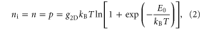
  the absolute temperature, and Ef the Fermi level. From above equations, the electron density in the CB is
 ![$n={{g}_{{\rm 2D}}}{{k}_{{\rm B}}}T{\rm ln} \left\{ 1+{\rm exp} \left[ \left( {{E}_{{\rm f}}}-{{E}_{{\rm c}}} \right)/{{k}_{{\rm B}}}T \right] \right\}$](https://content.cld.iop.org/journals/2053-1583/2/1/015003/revision1/tdm507601ieqn29.gif) and the hole density in the VB is
and the hole density in the VB is ![$p={{g}_{{\rm 2D}}}{{k}_{{\rm B}}}T{\rm ln} \left\{ 1+{\rm exp} \left[ -\left( {{E}_{{\rm f}}}-{{E}_{{\rm v}}} \right)/{{k}_{{\rm B}}}T \right] \right\}.$](https://content.cld.iop.org/journals/2053-1583/2/1/015003/revision1/tdm507601ieqn30.gif) We make the assumption that the electrons and holes have the same effective masses, which may be relaxed if not appropriate. Under thermal equilibrium, the Fermi energy for n-type TMD layer is thus
We make the assumption that the electrons and holes have the same effective masses, which may be relaxed if not appropriate. Under thermal equilibrium, the Fermi energy for n-type TMD layer is thus ![${{E}_{{\rm f}}}-{{E}_{{\rm c}}}={{k}_{{\rm B}}}T{\rm ln} \left[ {\rm exp} \left( n/{{g}_{{\rm 2D}}}{{k}_{{\rm B}}}T \right)-1 \right],$](https://content.cld.iop.org/journals/2053-1583/2/1/015003/revision1/tdm507601ieqn31.gif) and for p-type it is
and for p-type it is ![${{E}_{{\rm v}}}-{{E}_{{\rm f}}}={{k}_{{\rm B}}}T{\rm ln} \left[ {\rm exp} \left( p/{{g}_{{\rm 2D}}}{{k}_{{\rm B}}}T \right)-1 \right]$](https://content.cld.iop.org/journals/2053-1583/2/1/015003/revision1/tdm507601ieqn32.gif) .
.
Figure 1(a) shows  plotted as a function of temperature for MoS2 single layers for different 2D carrier densities. The red lines are for n-type and the blue lines for p-type layers. The horizontal dashed line indicates the Fermi level for intrinsic MoS2; it stays at the mid gap because of the assumed symmetric bandstructure. SL TMDs have large electron effective masses, (∼0.57m0 for MoS2, ∼0.6m0 for MoSe2, and ∼0.61m0 for MoTe2) [12]. As a result, the DOS is high. As shown in figure 1(a), the carrier statistics stays effectively nondegenerate at room temperature over a very wide range of density of interest (1011 ∼ 1013 cm−2), with the Fermi level hardly entering the bands. As expected, at elevated temperatures the semiconductor turns intrinsic because of interband thermal excitation of carriers. The intrinsic carrier density
  in 2D crystal semiconductors is given by
where 
 is the band gap energy. Since in most 2D semiconductors,
  [12],
[12],  can be approximated by
 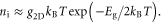 The intrinsic sheet carrier density is low even at room temperature because of the large bandgap, for example,
  ∼ 1.1 × 10⁻² cm−2 for SL MoS2 as compared to ∼1011 cm−2 for zero-gap graphene [8]. The carrier density in a semiconductor cannot be lower than ni at that temperature; this is also the reason for the high achievable on–off ratios in TMD FETs compared to 2D graphene.
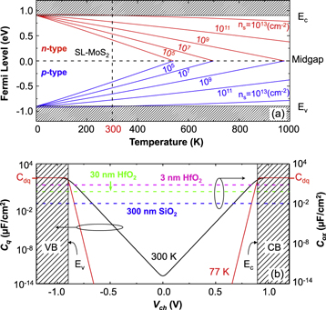
Figure 1. (a) Fermi level as a function of temperature for MoS2 single layers for different 2D carrier densities. Red lines show Fermi levels for n-type and blue lines for p-type MoS2 layers. The horizontal dashed line indicates the location of midgap and the vertical dashed line indicates the room temperature, 300 K. (b) The quantum capacitance  as a function of the local channel electrostatic potential
  at 77 and 300 K. The electrostatic capacitances per unit area of 3 and 30 nm HfO2, and 300 nm SiO2 are shown as references.
  is the degenerate limit of
  .
.
Download figure:
Standard image High-resolution imageThe effect of the gate voltage in a FET is to tune the carrier density, and consequently, the Fermi level in FET channels. A positive gate voltage applied to an intrinsic 2D crystal single layer channel populates the CB with electrons, and the Fermi level is driven from the midgap towards the CB edge. The local channel electrostatic potential  which is tuned by the gate bias, determines the electron density in the 2D crystal layer:
Writing the total charge density in a 2D semiconductor single layer  as a function of
  and using the definition of quantum capacitance
  one obtains for 2D crystals
Figure 1(b) shows the calculated quantum capacitance for SL MoS2 as a function of  at room temperature and 77 K. For intrinsic layers,
  in the figure also indicates the location of the Fermi level. The electrostatic parallel-plate capacitances
  (per unit area) for two dielectrics typically used as the gate oxide in TMD FETs: HfO2 and SiO2, are shown. Only when the Fermi level is deep inside the CB or VB, when
  and the quantum capacitance
  saturates and approaches the degenerate limit:
 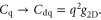 As indicated by the dielectric cases in figure 1(b), for most of the nondegenerate region,
  is much lower than
  For very thin dielectrics, for example: 3 nm HfO2, even the degenerate limit
  is comparable with
  Thus the quantum capacitance can significantly influence the field effect. Device models should include
  in order to properly capture the device behavior, especially in the subthreshold region and for devices with high-κ or thin dielectrics.When the quantum capacitance is taken into consideration, a part of the gate voltage is dropped in the channel to populate it with an electron (hole) density
 as shown in the equivalent circuit in the inset of figure 2(a). For FETs with intrinsic 2D semiconductor channels, under positive gate bias, the relationship between
  and
and  is
is
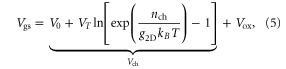
where  and
and  denote the voltage drops in the channel and the dielectric layer respectively, and
 and
and  Equation (5) is a transcendental equation, which can only be solved numerically. The resulting
  in an intrinsic SL MoS2 channel as a function of
  from equation (5) is shown in figure 2(a) as black lines for 3 and 300 nm SiO2 gate oxide. Electron densities calculated with equation (1) are also shown in figure 2(a) as reference with blue lines. The shaded areas and the arrows indicate the error between
  and
and  It is obvious that the carrier density can be strongly overestimated by using the commonly used expression equation (1) for
  The large deviation proves that neglecting the quantum capacitance will lead to significant errors in the extraction of the carrier density.
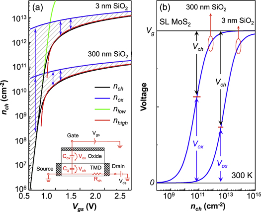
Figure 2. (a) Electron densities as a function of gate voltage: nch is the accurate electron density calculated with the transcendental equation equation (5); nox is the electron density obtained from equation (1); nlow and nhigh are the approximated solutions to equation (5) at low and high gate bias respectively. The shaded areas and the arrows indicate the error between nch and nox. The equivalent circuit of the device is shown in the inset. (b) The proportions of Vch and Vox in Vg as a function of  for SL MoS2 FETs coating with 3 and 300 nm SiO2 gate dielectrics.
Download figure:
Standard image High-resolution imageReducing equation (5) from the transcendental form under common device operation conditions will enable the direct calculation of  At low gate voltages in the sub-threshold region of a FET where
  most of the gate voltage drops in the channel, that is
  In this case, the electron density in the channel
  reduces to
as shown by the green line in figure 2(a).  arises solely due to the channel material itself, thus is independent of the gate oxide. At high gate voltages when the FET is 'strongly on',
  reaches
  the channel electron density
  is approximately

as shown by the red lines in figure 2(a).  is the critical gate voltage that differentiates the situations described by equations (6) and (7), which corresponds to the gate voltage when
  ,
,
When 
 is determined by equation (6); when
 is determined by equation (7). The critical carrier density
  corresponding to
  is
is
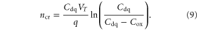
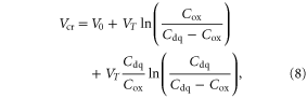
For SL MoS2 FETs with 300 nm SiO2 gate oxide,  and
and  ∼ 1.86 × 109 cm−2; for 3 nm SiO2,
  and
and  ∼ 1.87 × 1011 cm−2. It is worth noting that equations (3)–(8) are obtained based on the intrinsic material and the assumption of zero flat-band voltage, that is,
  If a SL MoS2 is unintentionally doped with n-type impurities (which is typical till date),
  shifts by several tens of Volts toward negative values depending on the impurity density and the gate barrier thickness. In this case, the gate voltage term
  in equations (6) and (7) should be replaced by
  .
.
Now we discuss the validity of using equation (1) to estimate the carrier density in the 2D crystal FET channel. Because equation (1) is valid only when  we show the proportions of
  and
and  in
in  as a function of
  obtained from equation (5) for SL MoS2 FETs with 3 and 300 nm SiO2 dielectric layers in figure 2(b). As can be observed, for FET with 300 nm SiO2 dielectric layer,
  ranging from 1011 to 1013 cm−2 can easily be overestimated by equation (1) because Vox is significantly smaller than
  For the very thin 3 nm SiO2 gate oxide,
  can be strongly overestimated over the whole carrier density range of interest: 1011 ∼ 1013 cm−2, as also shown in figure 2(b). For thin gate barriers, a significant amount of voltage is dropped in the semiconductor channel because of the carrier statistics, and its neglect can cause large errors.
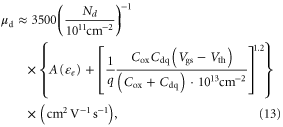
With the correct carrier statistics, we now re-examine the methods employed to extract other important parameters from the device characteristics, for example, the carrier mobility. A commonly used method to estimate the carrier mobility in the channel is the field-effect mobility  given by [9, 13–17]:
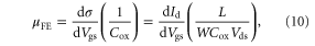
where σ is the electronic conductivity in the channel,  is the drain current,
  is the drain voltage, and
  and
and  are the length and width of the channel respectively. Equation (10) is widely used in device analysis of Si-based MOSFETs and III-V semiconductor-based FETs. However its validity in TMD devices must be re-examined. Equation (10) is derived from the fundamental drift current equation of an FET in the linear regime at small drain voltages:
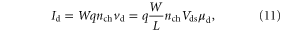
where  and
and  are the carrier drift velocity and drift mobility in the channel respectively. To obtain equation (10) from equation (11), the first assumption is that the carrier density in the channel can be calculated using equation (1). For on-state device operation where
  equation (7) captures the carrier statistics and quantum capacitance more accurately. The term
  or
or  can be eliminated by taking the derivative of
  versus
  Equation (10) can be recast as

which amounts to replacing  which is not a fundamental new result in itself, but we emphasize that not doing so can cause significant errors. However, another implicit but more important assumption in equations (10) and (12), which is barely discussed, is that the carrier mobility
  in the channel does not change when gate bias is varying. The derivative in equations (10) and (12) can lead to significant errors when
  is
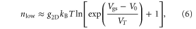
is  dependent, as we now discuss.Because the carrier density is modulated by the gate bias, the
  of
of  is determined by the dependence of
  on the carrier density
  Figure 3(a) shows the calculated electron drift mobility in SL MoS2 as a function of electron density at three different temperatures: 4, 77 and 300 K. The gate dielectric is chosen as 300 nm SiO2. The mobility is calculated in the relaxation-time approximation of the Boltzmann transport equation. Scatterings by polar optical phonons, deformation potential phonons (acoustic and optical), remote optical phonons from the dielectric layer, and ionized impurities have been taken into consideration. Details of the calculation can be found in [3]. As can be seen from figure 3(a), at all three temperatures,
  first increases with
  and then tends to saturate at high density. At high temperature, a higher carrier density is required to fully screen Coulombic scattering potentials. For example,
  starts to saturate at ∼3 × 1013 cm−2 at 300 K, but at ∼4 × 1011 cm−2 for very low temperature 4 K. Combining the results of figure 3(a) and equation (5), one can obtain the electron mobility as a function of
  as shown in figure 3(b). An ionized impurity density
  of 4 × 1012 cm−2 is assumed to be located in the channel, which leads to a negative shift of the threshold voltage of ∼55 V from the intrinsic case based on the following relationship:
  At 4 K, the mobility starts to saturate at
  while mobilities at 77 and 300 K keep increasing even when
  is well over 100 V. Note that the drift mobility
  discussed here differs from the Hall mobility
  by a Hall factor, which is induced by the magnetic field in the Hall-effect measurement. The Hall factor is often assumed to be unity, however careful consideration of the Hall factor with relevant scattering mechanisms at different temperatures needs further detailed study[18]. Baugher et al [19] have compared
  and
and  and found that
  can differ significantly from
  They attributed the lower
  to the possible screening of charged impurity scattering at higher densities, which is consistent with our results in figure 3. In the following, we quantitatively explain the discrepancy between the conventional method of extracting the field-effect mobility
  and the 'true' drift mobility
  in the channel by combining a theoretical transport calculation with density-dependent mobility, and with the correct electrostatics of the FET incorporating the correct carrier statistics and quantum capacitance. This final analysis explains the measured experimental behavior of SL TMD FET, and highlights the problems with conventional models of mobility extraction.

Figure 3. Calculated electron drift mobilities at three temperatures: 4, 77 and 300 K, as a function of (a) carrier density and (b) gate voltage.
Download figure:
Standard image High-resolution imageFigure 4(a) shows the experimentally obtained output characteristics (open squares) at gate voltages of 40, 0 and −40 V of a typical back-gated SL MoS2 FET with a 300 nm SiO2 layer as the gate oxide [15]. Figure 4(b) shows the transfer characteristics of the same device in both linear and log-linear plots at a fixed drain bias of 10 mV, the effect of the contact resistance has been de-embedded by using the experimental values [15]. Here we make the assumption that the contact resistance does not change with the gate voltage. The measured room temperature data are chosen for the study here because the contact effects play a less important role at higher temperature. The length and width of the channel are 4 and 9.9 μm respectively. Since the drain voltage is small, the variation of the carrier density and mobility from the source to the drain is ignored. Following the compact model proposed by Jiménez [20], the device characteristics in figure 4 are first modeled by assuming a constant mobility. The calculated currents are shown as solid black lines in figures 4(a) and (b). The carrier statistics are obtained from equations (3)–(5). As can be observed, with constant mobility, the on-state current appears to fit well for high  However, significant quantitative and more importantly, qualitative discrepancies are observed at low
  On the contrary, if we fit the current at low
  we would see large errors at high
  Thus we remodeled the devices characteristics by taking both the carrier statistics, and the
  of the electron mobility into account. This calculation is shown as red lines in figures 4(a) and (b). The impurity density is used as the fitting parameter, with value of ∼4 × 1012 cm−2. The excellent fit of the
 model to the experimental data over several orders of magnitude change in current indicates that if we use equation (10) or even equation (12) to extract the field-effect mobility from the FET transfer characteristics, we will be in significant error. Both the quantum capacitance and the density-dependent mobility must be included for proper extraction.
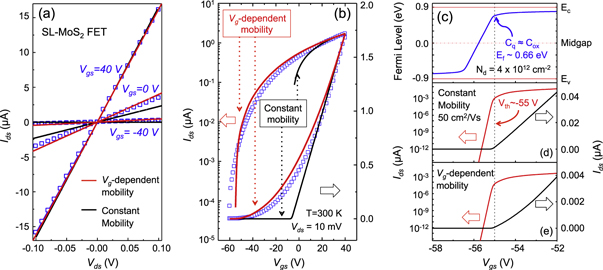
Figure 4. (a) Experimental output characteristics (open squares) of a typical back-gated SL MoS2 FET from [15]. (b) Transfer characteristics from the same device in both linear and log-linear plots. The solid black lines show the calculated output and transfer curves with the assumption of constant electron mobility while the solid red lines are calculated with  electron mobility. (c) Fermi level in the channel as a function of the gate voltage. (d) and (e) show the calculated transfer characteristics with assumed constant and
  electron mobility, respectively.
Download figure:
Standard image High-resolution imageFigures 4(c)–(e) show the calculated room temperature Fermi level in the SL MoS2 channel, transfer characteristics with constant and  mobilities respectively. The device structure is the same with that in figures 4(a) and (b) and
  is fixed at 4 × 1012 cm−2. In the sub-threshold region, the drain current is dominated by the carrier density increasing with
  Thus the threshold voltage
  can be defined as the voltage when the transfer characteristic curve has the highest curvature, as shown by the vertical dashed line in figures 4(c)–(e).
  distinguishes the sub-threshold region and the on-state region that described by equations (6) and (7) respectively. For current structure,
  is ∼−55 V. To further prove the validity of the method of extracting
  we find that when
 is located ∼0.66 eV above the midgap, as shown in figure 4(c). This is also the Fermi level when
  as can be observed in figure 1(b). Once the threshold voltage is extracted, one can now estimate the carrier drift mobility in the channel at room temperature with combining the empirical expression proposed in [3] and equation (7) for
  1013 cm−2:
where  is a fitting constant depending on
  for single-gated MoS2 FET with SiO2 gate oxide,
  is ∼0.036 [3].
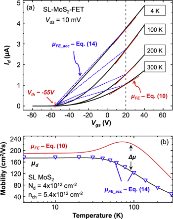
To further show the discrepancy between the field-effect mobility and the drift mobility in the device channel, we calculate the transfer characteristics of a SL MoS2 FET as a function of temperature, using the same parameters as used in figure 4. The example transfer curves at temperatures 4, 100, 200 and 300 K are shown in figure 5(a). Because  is usually extracted from the measured transfer characteristics in the region that appears to be linear [15], for example, for
  in figure 4(b), here we take the carrier mobility at
  as a case study. The carrier density at
  is
is  ∼ 5.4 × 1012 cm−2. The field-effect mobilities calculated using equation (10) are shown by the red line in figure 5(b). Because of the derivative term in equation (10),
  is proportional to the slope of the tangent to the
  –
– curve, as indicated by the red lines in figure 5(a). The black curve in figure 5(b) shows
  calculated using our transport model. As we can see from figure 5(b),
  is higher than μd over the entire temperature range. Moreover, the error
 is not constant as the temperature varies. The value of
  depends on the dependence of
  on
on  as was shown in figure 3(b). The faster
  increases with
  the higher is the discrepancy
 calculated by equation (10) shows a much higher value of ∼104 cm2 V−1 s−1 at 300 K while
  is ∼50 cm2 V−1 s−1. Conversely at 4 K, since
  starts to saturate at very low
 (∼190 cm2 V−1 s−1) is only slightly higher than
  (∼175 cm2 V−1 s−1). At temperature lower than 20 K, one can approximate
  with error less than 10%. Over 20 K,
  first increases and then decreases with increasing temperature, leading to an apparent increase of
  at temperatures ranging from ∼30 to ∼80 K. This observation can partially explain the experimentally obtained decrease of the field-effect mobility as the temperature is lowered [9]. Thus we conclude that
  extracted from the device transfer characteristics by equation (10) not only overestimates the electron mobility, but can also show a false temperature dependence. The red line in figure 5(b) shows an anomalous increase of mobility with temperature for 30 K <
  This is not related to any real scattering mechanism, but rather has roots in using incorrect carrier statistics.
Figure 5. (a) Calculated transfer characteristics (black lines) of a SL-MoS2 FET at temperatures 4, 77, 200 and 300 K. The red and blue dashed lines indicate the field-effect mobility obtained from equations (10) and (14), respectively. (b) Field-effect mobilities at  obtained from equations (10) and (14) as well as the drift mobility
  as functions of temperature.
Download figure:
Standard image High-resolution image
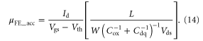
To accurately extract the carrier transport properties from the device measurements, the field-effect mobility may be obtained by:
 extracted from the calculated transfer curves in figure 5(a) using equation (14) are shown as open triangle symbols in figure 5(b) with
  taken as −55 V. We can see a very good agreement between
  and
and  Now
Now  is proportional to the slope of the straight line joining
  to
to  as indicated in figure 5(a) by blue dashed lines. Comparing the slopes of the blue and red lines in figure 5(a), one can easily see the error induced by equation (10). Note that the estimation performed here should be used under the assumption of perfect Ohmic contact (or after contact resistance has been effectively eliminated). For current TMD semiconductors, it is still a challenge to obtain Ohmic contacts with high transparency. TMD FETs with the same channel material but with different contact metals can show very different electrostatic characteristics, and thus will give false information of the channel carrier statistics and mobillities [21–23]. A number of efforts have been made to improve the contact [16, 24–28], and remarkable low contact resistances have been achieved [29–31].
In conclusion, we have investigated the importance of the carrier statistics and quantum capacitance in understanding the characteristics of 2D crystal semiconductor electronic devices. The commonly used expressions for extracting the carrier density and field-effect mobility from the transfer characteristics of 2D semiconductor FET are demonstrated to be only valid for very limiting conditions, and prone to severe errors. By combining the correct carrier statistics, quantum capacitance, and density-dependent mobitlities, we prescribe a new method to extract the correct mobilities from the FET measurements. The results presented here are expected to be useful to place our understanding of the fundamental properties of 2D crystal semiconductors on a more firm foundation.
Acknowledgments
The authors thank Deep Jariwala, Dr Vinod K Sangwan, and Dr Mark C Hersam for fruitful discussions and for sharing experimental data. The research is supported in part by an NSF ECCS grant monitored by Dr Anupama Kaul, AFOSR, and the Center for Low Energy Systems Technology (LEAST), one of the six centers supported by the STARnet phase of the Focus Center Research Program (FCRP), a Semiconductor Research Corporation program sponsored by MARCO and DARPA.