
Abstract
We review current challenges and perspectives in graphene spintronics, which is one of the most promising directions of innovation, given its room-temperature long-spin lifetimes and the ability of graphene to be easily interfaced with other classes of materials (ferromagnets, magnetic insulators, semiconductors, oxides, etc), allowing proximity effects to be harvested. The general context of spintronics is first discussed together with open issues and recent advances achieved by the Graphene Spintronics Work Package consortium within the Graphene Flagship project. Based on such progress, which establishes the state of the art, several novel opportunities for spin manipulation such as the generation of pure spin current (through spin Hall effect) and the control of magnetization through the spin torque phenomena appear on the horizon. Practical applications are within reach, but will require the demonstration of wafer-scale graphene device integration, and the realization of functional prototypes employed for determined applications such as magnetic sensors or nano-oscillators. This is a specially commissioned editorial from the Graphene Flagship Work Package on Spintronics. This editorial is part of the 2D Materials focus collection on 'Progress on the science and applications of two-dimensional materials,' published in association with the Graphene Flagship. It provides an overview of key recent advances of the spintronics work package as well as the mid-term objectives of the consortium.
Export citation and abstract BibTeX RIS
Introduction
Spintronics has emerged from discoveries in the 1980s concerning spin-dependent electron transport phenomena in solid-state devices. Following the observation of spin-polarized electron injection from a ferromagnetic metal to a normal metal by Johnson and Silsbee (1985) [1], the foundational step of the field of spintronics has been the scientific discovery of giant magnetoresistance in thin-film structures composed of alternating ferromagnetic and non-magnetic conductive layers by Albert Fert et al [2] and Peter Grünberg et al [3]. The use of the spin degree of freedom transferred over nanoscale distances to control the magnetoresistance of a device has required the use of various types of magnetic and non-magnetic metallic and semiconducting materials, and has resulted in a massive technological impact in magnetic field sensors, which are used to read data in hard disk drives, biosensors, microelectromechanical systems (MEMS) and magnetoresistive random-access memories (MRAM) [4]. The field of spintronics is now witnessing a second revolution after the discovery of the spin transfer torque effect, which permits the control of the magnetization with electrical current [5].
Since 2004, the fabrication of a two-dimensional one atom thick carbon membrane, better known as graphene [6, 7], has captivated an endlessly growing community of scientific experts focusing on a large, diverse list of exceptional physical properties and the applicative potential of this unique material [8].
Graphene spintronics was envisioned early on as a promising direction for work and innovation, owing to the combination of the unique electronic band structure of so-called massless Dirac fermions, weakly sensitive to backscattering and travelling at very high speed over very wide distances at room temperature. In addition, the weak spin–orbit coupling (SOC) in sp2 carbon also suggested that electron spin should be carried nearly unaffected over unprecedented distances, making feasible practical applications of lateral spintronics [9, 10]. Pioneering works initially echoed such high expectations [11], while more recent experimental results have confirmed the potential of graphene for transporting spin signal at room temperature over tens of micrometers, which is more than enough for technological realization [12–14].
Graphene spintronics (GS) is one of the fundamental topics of the Graphene Flagship consortium. The global objective of the Graphene Spintronics Work Package (GS-WP) task force is to establish the ultimate scientific and technological potential of graphene and graphene-related materials for spintronics. It targets efficient spin injection, transport and detection and also aims at demonstrating spin gating and spin manipulation in graphene spintronic devices. The ultimate goal is to realize operational devices for information storage and information processing, by engineering device architecture and material transformations.
To progress in the demonstration of practical applications, the consortium is benchmarking various forms of graphene (suspended, supported on oxide and boron-nitride substrates or fully encapsulated) for achieving the best spin injection, propagation and detection functions. During the first year of its operation, given the complexity of the problem at hand, several directions of work have been engaged by the consortium from both theoretical and experimental perspectives, constructing synergies and progressively clarifying existing controversies.
Recent progress of the Graphene Spintronics Flagship consortium
On the experimental side, the GS-WP consortium has already reported world record spin lifetimes of various forms of supported graphene spin valve devices, increased by several orders of magnitude with respect to prior state-of-the-art technology and obtained through transversal optimization of material quality and device integration processes.
The contact effects and general device environmental factors on the estimated spin relaxation lengths have been analyzed in detail. In 2000 the so-called conductivity mismatch was identified as an important factor that could influence and reduce, or even completely suppress, spin injection from ferromagnets into semiconductors [4]. It was shown that the resistance of the contacts should be higher than the spin resistance of the medium in which the spins are injected, to prevent the backflow of the spins into the contact. This backflow would be accompanied by spin relaxation in the metallic ferromagnet (which has a very short spin relaxation time), thus reducing the spin injection efficiency. It was shown that this had to be balanced with the dwell time of the spins in the semiconductor channel, giving only a narrow window for the contact resistance in devices [15].
The importance of using high-resistance contacts in graphene spin valves was established early on by a member of the consortium [12], but an experimental link between the effective spin relaxation time extracted from Hanle spin precession measurements (see the typical Hanle curve in figure 1(b)) and the values of contact resistances was provided in 2014 [13–19]. This identifies the above mechanism as one of the factors that could be responsible for the observed short spin relaxation times. Another bottleneck for spin transport is inhomogeneous oxide barriers which may result in conducting pinholes within the otherwise insulating spin injection and detection barriers. In graphene/MgO/Co spin-valve devices it was found that the pinholes cause inhomogeneous current flow through the MgO barrier. Next to the actual spin signal, this results in an additional charge accumulation signal which is measured as a magnetic field–dependent background signal in the non-local voltage [19]. This background signal, which is often observed in non-local spin transport studies, is thus a hallmark for the quality of the oxide barriers.
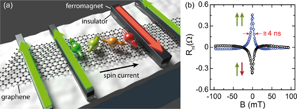
Figure 1. (a) Schematics of the typical four-terminal spin valve geometry for measuring spin lifetime in graphene samples. (b) Hanle experimental curve from which spin lifetimes are extracted using a semiclassical spin diffusion equation. Reprinted with permission from [14]. Copyright 2014 American Chemical Society.
Download figure:
Standard image High-resolution imageSpin transport was studied in non-local spin valve field effect devices (see figure 1(a)), where the graphene was attached to, or supported by, a hexagonal boron nitride (hBN) [14, 20]. A significant increase of the spin lifetime (exceeding 3 ns, figure 2(b)) and length (exceeding 10 micrometres at room temperature) was reported as compared with graphene on SiO2. Other performed experiments where the graphene layer was fully encapsulated by using hBN layers showed that the ratio of spin lifetimes for spin directions perpendicular and parallel to the graphene sheet can be tuned by the use of top and bottom gate electrodes (figure 2(a)). These results are in agreement with an electrically induced Rashba-type spin–orbit coupling and open up new possibilities for electric control of spin transport in graphene. Second, by using a careful procedure to eliminate the effects of the non-encapsulated outer regions, values above 12 micrometres were obtained for the spin relaxation length in the central encapsulated region, thus establishing a new record for spin relaxation length at room temperature [13].

Figure 2. (a) Evolution of the ratio between in-plane and out-of-plane spin lifetimes versus applied perpendicular electric field for different carrier densities (adapted from [13]). (b) Spin lifetimes versus charge mobility for various types of graphene (single layer (SLG), bilayer (BL), trilayers (TL)) and substrates (hBN and SiO2). Red data points are included from [13]. Reprinted with permission from [14]. Copyright 2014 American Chemical Society.
Download figure:
Standard image High-resolution imageOn the theoretical side, the first fundamental question is to understand the origin of the discrepancy between state-of-the art experimental values and the original predictions of spin lifetimes of around a microsecond, based on conventionally conceived mechanisms of spin relaxation and heralding graphene as an exceptional (and unique) material for the development of lateral spintronics [21]. After almost a decade of experimental efforts to improve the quality of the material and device fabrication, spin lifetime remains many orders of magnitude shorter (from 3 to 6 or even more!) in the nanosecond scale.
Uniting different modelling scales (from ab initio to efficient real space spin propagation methods), the consortium has unravelled relaxation mechanisms which make spin dynamics in graphene unique, demanding fully coherent quantum dynamics treatment beyond conventional and semi-classical spin Bloch-type approximations. One remarkable achievement is the understanding of new spin relaxation effects in graphene which contribute to clarifying why spin lifetimes appear shorter than initially anticipated; more precisely, these are two novel spin relaxation mechanisms related to the presence of magnetic moment or spin–pseudospin entanglement.
The first one identifies local magnetic moments sitting on resonant impurities as the culprits for the ultrafast spin relaxation seen in experiments [22]. The key is the combination of a spin flip due to the exchange interaction with local moments, and the resonant scattering. While in conventional scattering (Born approximation) the probability for a spin flip is small (say, 0.01%), at resonance the chance for a spin flip becomes comparable to that of spin conserving scattering (say, 50%). In resonance, the electrons are trapped for a certain dwell time on the impurity; the electron spin has more time to precess about the magnetic spin, effectively enhancing the exchange interaction which causes the precession (figure 3(a)). Such mechanism works as long as the spin precession time is longer or comparable to the resonance dwell time. It turns out that the dwell time is indeed longer than the precession time for ad-atoms such as hydrogen [22].

Figure 3. (a) 'Planetary' model of resonant scattering electrons tend to stay around ('orbit') the impurity for a certain dwell time. If the time is comparable or greater than the spin precession time due to the exchange interaction with the local moment on the impurity, the spin flip is as likely as non-spin flip. (b) Schematics of the entangle spin–pseudospin dynamics induced by local Rashba spin–orbit interaction related to adsorbed gold atoms.
Download figure:
Standard image High-resolution imageThe description of the local magnetism has been further extended using the self-consistent Hubbard model in the mean field approximation (for the dilute limit), while spin relaxation lengths and transport times were computed using an efficient real space order N wavepacket propagation method [23]. Typical spin lifetimes on the order of 1 ns are obtained for 1 ppm of hydrogen impurities whereas transport time of about 50 ps leads to spin diffusion lengths far beyond tens of micrometres. The scaling of spin lifetimes with impurity density is here described by the Elliott–Yafet mechanism [24].
A second new relaxation mechanism discovered by the consortium is related to the complex interplay between spin and pseudospin quantum degrees of freedom when disorder does not mix valleys [25]. Such strong contribution of spin/pseudospin entanglement is particularly important when defects or impurities at the origin of local Rashba spin–orbit coupling preserve the pseudospin symmetry and lead to a very long mean free path (schematics shown in figure 3(b)).
The pseudospin-related effects (and associated Berry's phase) are known to drive most of the unique transport signatures of graphene (Klein tunnelling, weak antilocalization, anomalous quantum Hall effect, etc) but until our study, the role of the pseudospin on the spin relaxation mechanism has been underestimated and not quantified. Pseudospin and spin dynamics are usually perceived as decoupled from each other, with pseudospin dynamics much faster than that for spins, with consequently much shorter pseudospin lifetimes. However, this picture collapses in the vicinity of the Dirac point, a region that is out of reach for semi-classical and perturbative approaches, despite being particularly relevant for experiments. Moreover, in the presence of SOC, spin couples to orbital motion, and therefore to pseudospin [26], so that spin and pseudospin dynamics cannot be treated independently.
The effect of weak perturbation induced by low densities of ad-atoms (down to 1012 cm−2 or lower) was analyzed with a fully coherent quantum dynamics treatment going beyond standard Bloch spin diffusion equations [25]. By introducing a random Rashba field in real space but vanishingly small intervalley scattering, long mean-free paths in the order of several hundreds of nanometres were obtained, while the study of wavepacket propagation and extraction of the time-dependent spin polarization revealed short spin lifetimes with an energy dependence in agreement with experimental data, exhibiting a minimum at the Dirac point. The spin relaxation mechanism revealed in the non-magnetic samples is interpreted as resulting from a quantum entanglement between spin and pseudospin driven by random SOC, which is unique to graphene. The mixing between spin- and pseudospin-related Berry's phase results in fast spin dephasing even when approaching the ballistic limit, with increasing relaxation times away from the Dirac point, as has been repeatedly observed experimentally. In the clean graphene limit, SOC can be caused by ad-atoms, ripples or even the substrate, thus opening possibilities for monitoring spin manipulation acting on the pseudospin degree of freedom. Such findings actually suggest inspiring ways to control the spin by modifying the pseudospin or vice versa. For example, spins could be manipulated by inducing pseudomagnetic fields by straining graphene [27].
More recently, the consortium has been working on the exploration of spin dynamics in ultraclean graphene devices and numerical results have shown that a very weak uniform Rashba spin–orbit coupling (with micron eV value), as generally assumed for supported graphene, in conjunction with substrate-dependent electron–hole puddles, yields spin lifetimes in the range of few hundreds of picoseconds to the nanosecond scale. The relaxation process in this clean limit is jointly governed by a Dyakonov–Perel together with a purely dephasing mechanism whose relative strength depends on the electron–hole puddle characteristics [28]. Spin dynamics in clean graphene on silicon oxide is found to be dominated by a Dyakonov–Perel mechanism, in contrast with the case of puddles for boron-nitride substrate (following what is observed in experiments; see figure 2(b)).
The theoretical task force is also working on carefully analyzing the formation of magnetic moments in graphene for different types of impurities and defects as presumably produced by ion irradiation or direct chemical functionalization. A study of the magnetic structure and SOC induced by hydrogen and fluorine ad-atoms and mono-vacancy in graphene has been performed and connected with spin lifetime calculation. The electronic structures of semi-hydrogenated, semi-fluorinated and defective graphene are investigated by means of first-principles techniques, which allow analyzing the complex interplay between SOC and local magnetism. Magnetic properties of vacancies in trilayer graphene have also been studied, showing stronger robustness of magnetism of single vacancies reacting with bottom and top layers, when compared to the case of single vacancies in isolated monolayers. First-principles calculations of large supercells of fluorinated graphene to complete the description of the dilute limit of fluorination, calculating the spin-flip scattering probabilities for hydrogen and fluorine ad-atoms, have revealed fundamental differences between both types of addends, with absence of magnetism in the case of fluorine, but giant spin–orbit interaction [29]. All those efforts in ab initio modelling are currently harvested to elaborate refined tight-binding models used for the study of spin dynamics, selecting the appropriate system for comparison with experiments done in the consortium. Further possibilities for inducing magnetism by means of magnetic insulator proximity effect are also explored both theoretically and experimentally [30]. For this purpose, particular attention is being paid to complex oxides such as ferrites and yttrium iron garnet with high Curie temperature.
Perspectives
One of the current challenges for the consortium is to characterize and optimize the fabrication technology for producing spintronic prototype devices based on large-area graphene (mainly CVD-grown polycrystalline graphene). This requires the study of device variability on the same integration chip, the clarification of the impact of grain boundaries on spin lifetimes and the achievement of long spin lifetimes. Although the electronic quality of the CVD form is compromised by the polycrystalline morphology which displays a variety of grain boundaries, scaffolds for chemical contamination [31], reasonable spin lifetimes of about 200 ps and spin diffusion lengths around 2 μm with channel lengths up to 4 μm have already been reported at room temperature [14]. In a recent development, the long-distance spin transport capability of CVD graphene with channels extending up to 16 μm on SiO2/Si substrates (figure 4(a)) has been demonstrated [16]. Non-local spin transport and Hanle precession measurements in such long channels give rise to a spin lifetime of 1.2 ns with room-temperature spin diffusion length of 6 μm (see figure 4(b)). Such long spin transport capability of CVD graphene opens up possibilities for lateral spintronic memory and logic technologies, and will be further extensively investigated by the consortium.
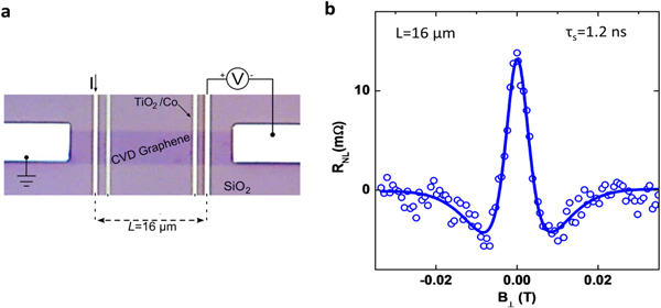
Figure 4. (a) Microscope image of a fabricated long-channel CVD graphene device on Si/SiO2 substrate with multiple ferromagnetic tunnel contacts for spin injection and detection in a non-local geometry. (b) Hanle spin precession measurement in a L = 16 μm long CVD graphene channel yielding spin relaxation time τs of 1.2 ns at room temperature. Adapted from [16].
Download figure:
Standard image High-resolution imageExperimental and theoretical efforts will be further maximized and a focus will be made on engineering efficient device fabrication techniques embedding spin manipulation functionality such as the spin Hall effect (SHE) [32] and spin torque, to produce practical (room-temperature) applications of graphene spintronic devices.
Spin current generation by means of the SHE in heavy metals for spin torque applications has gained great attention in recent years and magnetic memory prototypes have been demonstrated using this technology. Spin Hall angles larger than 10% have been recently reported in graphene after the addition of ad-atoms, metallic particles or by contacting graphene with WS2, suggesting that the SHE (in modified graphene) can also be an efficient way of generating spin currents [33]. These results have been achieved using the so-called Hall bar geometry (figure 5(a)) that relies on the SHE for spin injection and the inverse SHE for detection. The mechanisms involved in generating the detected signals are not clear and therefore full understanding and further optimization of SHE have not yet been achieved, and will be key objectives for the years to come. Another device geometry such as the one shown in (figure 5(b)) presents an alternative for the exploration and control of SHE in a modified graphene platform and will be investigated [34].

Figure 5. (a) Hall bar device. A charge current in the top arm generates a spin current via the SHE that flows to the bottom bar, which results in a measurable voltage via the inverse SHE. (b) Nonlocal device where the spin current is achieved via spin injection from a ferromagnet (dark electrode). Adapted from [32].
Download figure:
Standard image High-resolution imageTo implement strong enough spin–orbit coupling heterostructures of graphene with other 2D materials having large spin–orbit coupling, such as transition metal di-chalcogenides (TMD), is another target, since they offer larger capability to manipulate spin by electric field. The spin–orbit interaction can be characterized by non-local spin-Hall and spin-valve measurements. To benefit from the long spin transport in graphene and possibility of spin manipulation, TMD hybrid devices consisting of both materials as pictured in figure 6 are now a target of the consortium.
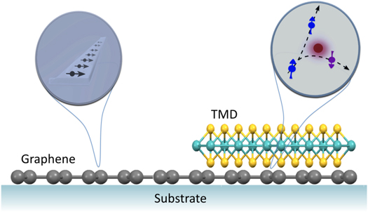
Figure 6. Schematics of graphene/TMD van der Waals heterostructures for spin polarized transport and manipulation by proximity-induced effects. The aim is to exploit the long spin coherence length of graphene and high spin–orbit coupling of TMDs/graphene interfaces in a single device.
Download figure:
Standard image High-resolution imageIndeed, for spin injection and detection in graphene, the conventional metal-oxide barriers such as Al2O3 and MgO together with ferromagnetic contacts are often used [9]. However, the growth of oxide barriers on graphene is challenging and suffers from problems such as pinholes, interface roughness and defects related to oxygen vacancies and doping in graphene under the contacts. The 2D nature of insulating hexagonal boron nitride (hBN) makes it appealing for spin-tunnel barriers because of the absence of surface states, which can minimize the charge or spin traps at the interface. Recently, large-area CVD-grown hBN has been explored by the consortium as a tunnel barrier for spin injection into both CVD graphene devices [16] and exfoliated graphene [35] (see figures 7(a), (b)). The tunnelling behaviour of CVD hBN and spin injection into graphene circumventing the conductivity mismatch problem has been demonstrated by the consortium [19, 35]. Figure 7(c) shows the non-local spin transport measurements in graphene employing Co/hBN tunnel contacts giving rise to spin polarization of 14% and spin lifetime of 0.5 ns in graphene. Similar results in terms of spin polarization and spin lifetimes have been obtained with Co/amorphous carbon contacts, which were patterned using electron beam induced deposition [36]. These contacts are able to sustain large injection currents without degradation (>109 A cm−2), resulting in spin accumulations exceeding several meV. All such recent progress will be harnessed to push forward the performances of 2D-based spintronic devices.

Figure 7. (a) Schematics of ferromagnet (FM)/hBN-graphene van der Waals heterostructures for spin injection and detection. (b) Microscope image of a fabricated graphene spin transport device with hBN tunnel barrier and multiple Co contacts. (c) Spin injection and detection experiment in graphene employing hBN/Co tunnel contacts in a non-local geometry. The Hanle spin precession measurements yielding a tunnel spin polarization P ∼ 14% and spin lifetime τs ∼ 0.5 ns in graphene. Adapted from [35].
Download figure:
Standard image High-resolution image
Graphene (including graphite) also has a strong potential for vertical geometry spintronic devices since it can efficiently filter one of two spin channels [37] or it can significantly improve interfacial spin polarization giving rise to high tunnel magnetoresistance values. An important next step is to explore the behaviour of non-collinear spintronic phenomena such as spin transfer torque, important for development of STT-MRAM and spin torque nano-oscillators (STNO) [38]. Magnetization dynamics properties play a key role for these devices and will also be explored. Magnetic properties of FM|graphene interfaces such as perpendicular magnetocrystalline anisotropy are also an important direction to pursue for the downscaling of spintronic devices. It is also important to explore STT-related phenomena for lateral and more complex geometries.
The chemical functionalization of graphene by heavy ad-atoms is also a research direction of interest, given the predictions of the formation of a quantum spin Hall effect (QSHE) [39], and the recent demonstration of multiple quantum phases induced by ad-atoms segregation, including the crossover from a QSHE to a SHE effect [40].
Finally, a new venue and hence new potential for graphene for spintronics has been unveiled. It concerns its use as an impermeable spin-filtering membrane in vertical magnetic tunnel junctions. It has been demonstrated that graphene layers directly grown by CVD on ferromagnets protected them from oxidation. This has not only unlocked simple low-cost wet/ambient processes for spintronics (e.g. atomic layer deposition), but has also led to the observation of novel strong spin-filtering phenomena at the graphene–ferromagnet interface [41].
Conclusion
The main scientific conclusions are as follows. First, the type of graphene used in spintronic devices (mechanically exfoliated, epitaxially grown or CVD grown) is important to achieve long spin diffusion lengths, but the preservation of its quality must be enforced by using encapsulation with hBN layers, or special treatments to avoid contact contamination, impedance mismatch or too-invasive substrate effects. Second, the theoretically revealed novel spin relaxation mechanisms (local magnetism and spin/pseudospin entanglement) suggest possible ways to further explore spin gating possibilities either by generating long-range magnetic ordering (for instance via the sublattice selective functionalization with hydrogen ad-atoms or other relevant species), or by using lattice deformations (strain) that are able to affect pseudospin degree of freedom and thus spin information.
All in all, the advances of the consortium are already demonstrating that graphene stands as a unique two-dimensional platform for technological co-implementation of data storage and information processing technologies on a common circuit platform, a longstanding and tantalizing quest for the spintronics field. The achievement of long spin lifetimes at room temperature has been essential, and the achieved values are now more than enough to allow researchers to work towards engineering of novel functional devices, in which efficient spin gating or manipulation functions (such as the formation and monitoring of pure spin currents and harnessing of the spin torque effect) will serve to create more sensitive and commercially competitive technologies such as magnetic sensors and nano-oscillators [38]. The GS-WP will now enter the phase of demonstrating the applicative potential of graphene for spintronics, while exploring the potential of other two-dimensional systems as complementary materials.
The challenges to overcome in order to demonstrate efficient technological integration of spin devices into competitive commercial applications are however significant, but the consolidated consortium gathering for the next phase (until 2018) has acquired a critical mass for moving forward in the established scientific and technology roadmap [8]. The elaboration of the essential building blocks during the H2020 EU-Flagship program should ultimately serve as a pathfinder for inspiring the creation of a much broader spectrum of spintronic devices for beyond CMOS (ultralow energy rewritable microchips, zero-power transistors and logic gates), while being compatible with more-than-Moore CMOS and non-volatile low energy MRAM memories.
Acknowledgments
The research leading to these results has received funding from the European Union Seventh Framework Programme under grant agreement number 604391 Graphene Flagship.