

Abstract
Multilayer InSe with a thickness above ∼20 nm, is a direct semiconductor with a peak absorption wavelength approaching λ = 1000 nm, which is a promising candidate for solar-energy conversion and 2D optoelectronics devices. We present herein the experimental observations of thickness-dependent conductivity and photoconductive-responsivity spectrum in multilayer InSe as well as optically enhanced transconductance gain in the multilayer InSe metal-semiconductor-field-effect transistor (MESFET) illuminated by a halogen lamp. The voltage-current (V-I) measurement result shows multilayer InSe belongs to a p-type semiconductor, which can form a p-channel FET device. Thickness (t) dependent conductivity (σ) of multilayer InSe reveals about six-order variation from 5076 (Ω-cm)−1 (t = 5 nm) to 2.56 × 10⁻³ (Ω-cm)−1 (t = 184 μm, bulk) following a relationship of σ ∝ t−1.38. The highest conductivity in a thin InSe (e.g. t = 5 nm) is due to the increase of carrier density when the thickness is decreased. The photoresponsivity spectrum of a Ag-InSe-Ag multilayer photoconductor demonstrates a prominent peak absorption at 1.1 ∼ 1.3 eV, matches well with the direct-free-exciton energy of the InSe. A multilayer p-InSe MESFET was tested by V-I measurement. The transconductance was measured and determined to be 
 The gm value will enhance about three times when the MESFET was placed under the illumination of a tungsten halogen lamp of a lower power density ∼0.5 mW · cm−2. All the experimental results demonstrate multilayer InSe a promising 2D material available for microelectronics and optoelectronics applications.
Export citation and abstract BibTeX RIS
1. Introduction
Recently 2D layered materials reveal great promise for the implementation of next generation planar nano-electronics and nano-optoelectronics devices after the silicon era. The layered semiconductor usually has a band gap (excepting graphene), and presents diverse and largely unexplored specific properties, which will show very different characteristics when the layer thickness varies from bulk to monolayers. The advantage of 2D semiconductor is its ultrathin thickness can be obtained from van-der-Waals separation of layers, which reveals atomic flatness with decreasing dangling bond and reducing surface roughness, therefore enhancing carrier mobility of electrical transport. The ultrathin thickness and significant reduction of surface roughness enhance electrostatic gate control, and promote the operation speed by the enhancement of carrier mobility. A number of studies have been carried out on field effect transistors (FET), wherein the central building element for performing integrated circuits (IC) is the use of monolayer or multilayer as the conduction channel of carrier transport [1–4].
Thickness effect is an important topic for recent 2D materials study. Nowadays there are mainly two groups of layered-type chalcogenides of most interest: transition-metal dichalcogenides (TMDCs) used for photodetection and integrated electronics (e.g. MoS2 [5], WSe2 [6], and ReS2 [7]) and III-VI layered semiconductors available for detector, optical memory, photo-emitter, field-effect transistor, and photovoltaic applications (e.g. In2Se3 [8–10], GaSe [11, 12], and InSe [13, 14]). For the TMDCs, MoS2 and WSe2 are generally indirect semiconductors. They are not suitable for luminescence devices in their bulk or multilayer form. More interest in the TMDCs system is partly because their band gaps can be adjustable to render an indirect-to-direct gap transition with changing their thickness approaching 'monolayer'. On the other hand, for the III-VI compounds, GaSe and InSe possess bulk- and multilayer-forms are essentially direct semiconductors, the direct band gaps are ∼2.0 eV and ∼1.24 eV, respectively [12, 13]. The advantages of direct 2D III-VI layer semiconductors are high carrier mobility, high optical-absorption coefficient, light emission, and they are even not necessary to mechanically exfoliate to get monolayers. Multilayer InSe with a thickness above 20 nm has been proven to be a direct semiconductor [15] possessing direct band gap close to 1 eV. It shows better infrared absorption range of sunlight spectrum with respect to that of GaSe. Thickness and optical effects on the conductive properties of the multilayer InSe are important for further fabrication in InSe multilayer 2D electronics and optoelectronics devices and which need further explore.
Chemical-vapor-transport (CVT) grown layered-chalcogenide crystals have been proven to possess high quality used in fundamental characterization as well as in fabrication of 2D nanodevices [16, 17]. In this work, we grew InSe layered crystals by CVT method using ICl3 as a transport agent. Several experiments including micro-photoluminescence (μ-PL), micro-Raman (μ-Raman), piezoreflectance (PzR), and photoconductivity (PC) measurements are implemented for studying fundamental properties of the InSe layered crystal. The μ-PL and μ-Raman signals of a multilayer InSe (∼90 nm thick) are simultaneously got from a micro-Raman spectrometer. The result shows an emission wavelength ∼1000 nm (from μ-PL) and two-layer-hexagonal (2H) structure (from μ-Raman modes) in the multilayer InSe. The direct band gap of multilayer InSe has been characterized from 20 to 325 K using PzR. The temperature dependence of direct band gap of InSe is analyzed. The result shows good crystal quality and better semiconductor performance of the as-grown InSe multilayer crystal. Photoconductive responsivity spectrum reveals peak-absorption energy of multilayer InSe is near 1.1–1.3 eV. It matches well with the direct band gap of indium selenide. Two additional features Es and E1 that coming from the transitions of defect and valence-band (EV) splitting have also been detected. Thickness-dependent conductivity measurements of multilayer InSe show the conductivity increases approximately six orders with thinning out the sample thickness from bulk to ∼5 nm. The mechanism for thickness-dependent resistivity change of InSe is discussed. A multilayer InSe metal-semiconductor-field-effect transistor (MESFET) made by silver contacts was implemented. The transistor voltage-current (V-I) characteristic with self-bias configuration of the MESFET under different conditions of dark and white-light illumination have been respectively tested. The result shows about three times amplification of transconductance for the photo-MESFET under the illumination of a tungsten halogen lamp with low light-power density of ∼0.5 mW · cm−2. Analog-circuit design of the self-bias multilayer InSe photo-MESFET demonstrates a prototype for future implementation of multilayer InSe micro- & opto-electronics.
2. Experimental section
The layered single crystals of InSe with different area size and thickness were grown by CVT method [13, 18] using ICl3 as a transport agent. The compounds of the crystals were prepared from the elements (In: 99.9999% pure and Se: 99.999%) by reaction at 600 °C for 2 days in evacuated quartz ampoules. To improve stoichiometry, selenium with 1 mol% in excess was added with respect to the stoichiometric mixture of the constituent elements. About 10 g of the elements together with an appropriate amount of transport agent (ICl3 about 10 mg cm−3) were introduced into a quartz ampoule (22 mm OD, 17 mm ID, 20 cm length), which was then cooled with liquid nitrogen, evacuated to 10−6 Torr and sealed. The mixture was slowly heated to 600 °C. This slow heating is necessary to avoid any explosions due to the strongly exothermic reaction between the elements. For crystal growth, the chemical transport was achieved by adding appropriate amount of synthesized material together with the transport agent placed inside a quartz tube. The growth temperature was set as 600 °C (heating zone) → 500 °C (growth zone) with a gradient of −5 °C cm−1. The reaction kept 240 h for producing single crystals. After the growth, the synthetic InSe crystals essentially have a hexagonal shape with the size areas ranging from ten to hundreds μm2. Some of them are even higher to several mm2. The as-grown microplates show black and shiny surface. The thickness of the microplates is from tens to hundreds μm. The weak van der Waals bonding between the layers means that the layered InSe can be separated (to ∼nm) from the c plane using Scotch tape with mechanical exfoliation.
The μ-PL & μ-Raman spectrum of the multilayer InSe was simultaneously measured from an integrated micro-Raman-PL identified system equipped with one 532 nm solid-state diode pumped laser as the excitation source. An objective lens (50x) of working distance ∼8 mm equipped in a microscope, acted as the inter-connection and coupled medium among sample, incident and scattered laser beams, and charge-coupled-device (CCD) spectrometer. The measurement range of μ-Raman & μ-PL spectrum was from the lowest cutting edge ∼2.323 eV lowered down to ∼1.133 eV with a spectral resolution of ∼0.4 meV. The incident power of the 532 nm laser was adjustable, from 0 to 100 mW with a focus spot size of ∼4 μm. The PzR experiments were carried out in the energy range of 1.15 to 1.38 eV. A 150 W tungsten halogen lamp filtered by a PTI 0.2 m (600 grooves/mm) monochromator provided the monochromatic light. The reflected light of the sample was detected by HUV2000B photodiode and the signal was recorded via an EG&G model 7265 dual phase lock-in amplifier. The PzR measurements were achieved by gluing the thin multilyer specimens on a 0.15 cm thick lead-zirconate-titanate (PZT) piezoelectric transducer driven by a 100 Vrms sinusoidal wave at 200 Hz. The alternating expansion and contraction of the transducer subjects the sample to an alternating strain with a typical rms Δl/l value of ∼10−5. A RMC model 22 closed-cycle cryogenic refrigerator equipped with a model 4075 digital thermometer controller facilitates the temperature-dependent measurements from 20 to 325 K.
The PC measurement of multilayer InSe was implemented by measuring photocurrent via chopping the incident monochromatic light and detecting the incremental current simultaneously by means of a lock-in detection system. The two ends of the layered InSe sample were coated with Ag as the ohmic-contact electrodes. The magnitude of photocurrent was detected via the voltage drop across the load resistor R (110 Ω) which connected in series with the sample. A voltage of DC 30 V was supplied to the circuit and the chopping frequency of 20 Hz was chosen. The PC responses were measured and recorded via a lock-in amplifier. The same monochromatic system as that for PzR measurement can be used. The PC measurement was performed in the energy range between 0.7 and 2.2 eV. The measured PC spectrum of the multilayer InSe was converted into a photoconductive responsivity (A/W) spectrum via the calibration of a OPHIR optical power meter equipped with broadband high-sensitivity thermal sensor (wavelength 0.15–6 μm).
The thickness-dependent conductivity measurements were implemented using two-probe contact method. The experimental result comparing to four-probe contact conductivity to make sure the measurement results are approximately comparable and possess ohmic-contact behavior. Many of the multilayer InSe nano- and micro-flakes with different thicknesses were mechanically exfoliated from the bulk InSe crystals using Scotch tape, and then transferred onto a SiO2/Si substrate. The contacts of each specimen were fabricated by focus-ion beam (FIB) with deposited Pt as the contact electrodes. The thickness of each multilayer sample was estimated using atomic force microscopy (AFM). The V-I measurement was performed via a semiconductor parameter analyzer with the auxiliary of a probe station. For the V-I and Photo V-I measurements of the multilayer InSe MESFET (i.e. ID versus VSD), the voltage scanning range of the semiconductor parameter analyzer was set at −5 to 5 V. The measurements are respectively performed under dark and under white-light illumination with various gate biases ranging from −5 to 5 V. A tungsten halogen lamp (DC 3.8 V, 0.3 A) acted as the white light emulator. The power supply was about 1 Watt. The averaged power density of the halogen lamp was set at approximately 0.5 mW cm−2 via the monitor of an OPHIR optical power meter. The emission spectrum of the halogen lamp has been measured (i.e. not shown here), which reveals a black-body radiation with a main hump peak close to ∼1.8 eV. The main hump peak also decreases its intensity when the emitting spectrum approaching infrared range.
3. Results and discussion
Figure 1(a) shows the μ-PL and μ-Raman results of a thin multilayer InSe in one single spectrum ranging from 1.333 to 2.323 eV. The sample image and thickness of the multilayer InSe observed by microscope and AFM are also demonstrated in figure 1(b). The layer plane of InSe presents a clear angle of 60° between a and b axes, which reveals well-defined shape related to the hexagonal structure in figure 1(b). The thickness of the multilayer InSe estimated by AFM is around 90 nm and their size area is about 10–20 μm as shown in figure 1(b). As shown in the μ-PL & μ-Raman spectrum in figure 1(a), the energy region higher than 2.323 eV shows the excitation source of 532 nm solid state laser while the prominent peak at ∼1.24 eV and the series peaks between 2.1 and 2.323 eV are the band-edge emission peak (μ-PL) and those of Raman vibration modes of the multilayer InSe. The band-edge emission peak may come from free-exciton (FX, correlated with direct band gap Eg) luminescence [13, 19] with energy of E ≈ 1.24 eV (wavelength λ ≈ 1000 nm). The inset in figure 1(a) depicts the magnification of the Raman peaks of the multilayer InSe from 2.15 to 2.35 eV, wherein the corresponding wavenumber (cm−1) values of the Raman modes are calculated from the energy separation between the modes and the 532 nm laser. The peak at 114 cm−1 is the  mode with a relative vibration orientation of Se(↑)-In(↑)-In(↓)-Se(↓) normal to layer for the monolayer Se-In-In-Se fundamental unit [20]. A peak of ∼175 cm−1 related to the in-plane atomic movements of Se(→)-In(←)-In(→)-Se(←) is the E''(TO) mode [21], which can also be detected in the μ-Raman spectrum in figure 1(a). The observed peak mode at 225 cm−1 is A1 mode with the atomic moving direction of the indium atom opposite to the
  mode with Se(↑)-In(↓)-In(↑)-Se(↓). The other modes in the inset of figure 1(a) between 380 and 1000 cm−1 are the higher-order modes of the A- and E-related modes. The entire Raman-peak pattern in figure 1(a) verifies hexagonal layered structure of the multilayer InSe. Figure 1(c) shows high-resolution transmission electron microscope (HRTEM) image and selected-area-electron diffraction (SAED) pattern of the multilayer InSe. The a, b axes and the well-defined 60° angle of a hexagon (as those shown in the morphology picture of figure 1(b)) are also demonstrated in the HRTEM image in figure 1(c). The SAED pattern in figure 1(c) also reveals high crystalline quality by presentation in hexagonal dotted pattern of the multilayer InSe.
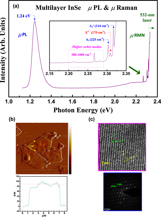
Figure 1. (a) The μ-PL & μ-Raman spectrum of multilayer InSe using 532 nm laser as the excitation source. (b) Sample image and thickness (measured by AFM) of the multilayer InSe used for μ-PL & μ-Raman measurement. (c) HRTEM image and SAED pattern of the multilayer InSe.
Download figure:
Standard image High-resolution imageIn order to verify the energy value of direct-band-edge transition and to estimate temperature-energy shift relation for a future InSe 2D device operated at higher temperature (>300 K), temperature-dependent PzR measurements of a multilayer InSe with thickness of ∼400 nm and area of ∼20 × 20 μm2 were carried out. Piezoreflectance (PzR) has been proven to be a very powerful tool for evaluation of optical transitions near band edge [22, 23]. The derivative spectral line shape of transition feature enhances the ability for determination of exact energy location of direct transition in semiconductors. Shown in figure 2(a) are the temperature-dependent PzR spectra of multilayer InSe in the temperature range between 20 and 325 K. The dashed lines are the experimental data, and solid curves are the least-square fits of the experimental data to a first derivative Lorentzian line-shape function appropriate for the band-edge excitonic feature expressed as [24]:

where A and  are the amplitude and phase of the line shape, and
  and
and  are energy and broadening parameter of the free-exciton (FX) transition in the multilayer InSe. The fits yield transition energies from 20 to 325 K are depicted with solid circles as shown in figure 2(b). As the general semiconductor behavior, the value of Eg decreases when the temperatures are increased. The energy value of the FX (Eg) at 300 K is about 1.237 eV, agrees well with the μ-PL result displayed in figure 1(a). The temperature-energy shift of band-edge transition of multilayer InSe can be generally analyzed using Varshni equation Eg(T) = Eg(0) − αT2/(β + T) [25], where Eg(0) is the band gap FX (Eg) at absolute zero, α is related to electron (exciton)-phonon interaction and β is closely correlated with Debye temperature [25]. The fitting result is shown by solid line in figure 2(b) and the obtained values of fitting parameters Eg(0) = 1.335 ± 0.001 eV, α = 0.57 ± 0.11 meV K−1 and β = 200 ± 100 K are displayed in figure 2(c). The temperature-energy shift speed of band gap of the multilayer InSe is similar to the other III-VI chalcogenide compounds of In2S3 [18] and GaS [23]. The result in figure 2(b) approximately displays a linear decrease of energy value of Eg with temperature higher than 200 K. The obtained Varshni fitting parameters in figure 2 provide a guideline estimate of band-gap change for a future multilayer InSe device operated at a temperature higher than 300 K.
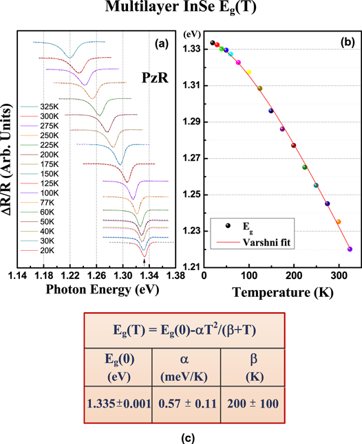
Figure 2. (a) Temperature-dependent PzR spectra of multilayer InSe in the temperature range between 20 and 325 K near band edge. (b) The dependence of temperature-energy shift of direct band-edge transition in multilayer InSe. The solid circles are the experimental Eg values and solid line is the fitting result using Varshni equation. (c) Values of fitting parameters obtained in (b) for the multilayer InSe.
Download figure:
Standard image High-resolution imageUnlike the other multilayer MoS2 and WS2 are indirect (i.e. thickness beyond monolayer), the multilayer InSe with thickness larger than ∼20 nm is a direct-band-gap semiconductor [15], which may own high mobility (∼1000 cm2/V-sec) [14], high optical-absorption coefficient and excellent luminescent efficiency [13]. To evaluate photoconductive responsivity property of the multilayer InSe layer crystal, PC measurement of a multilayer InSe with thickness ∼400 nm and area ∼0.01 mm2 was implemented in the energy range of 0.7–2.2 eV near band edge (i.e. in near infrared (NIR) region). Figure 3(a) shows the photoconductive responsivity spectrum of the multilayer InSe photoconductor converted from a broad band & thermo-type optical power meter (i.e. measured for the incident light). The inset in figure 3(a) depicts the representative scheme of photoconductivity measurement of the InSe multilayer. The corresponding ohmic-contact behavior of the photoconductor (with silver contact) is verified and displayed in figure 3(b). As shown in figure 3(a), the photoconductive responsivity spectrum of multilayer InSe reveals a prominent peak photoresponse (∼7.3 A W−1) at the energy region between 1.1 and 1.3 eV, matching well with the direct-band-edge FX (Eg) energy portion as measured in figures 1 and 2. There are also two additional peak features of ES and E1 present below and above band edge of multilayer InSe shown in figure 3(a). They are probably coming from the surface state and valence-band splitting (Se 4pxy) of InSe crystal [26]. The peak-like shape of ES, FX (Eg), and E1 (not shown step-like shape) in the photoconductive responsivity spectrum of multilayer InSe (see figure 3(a)) is maybe caused by surface-recombination effect of the photo-excited carriers owing to the existence of surface defects and surface states in the InSe. Figure 3(c) depicts the representative band scheme of the biased Ag-InSe-Ag photoconductor under the monochromatic light's illumination. The work function of silver is qΦm = 4.26 eV and electron affinity of InSe is about qχ = 4.55 eV, which will result in downward band bending in figure 3(c). The multilayer InSe belongs to a p-type semiconductor which may cause by indium vacancy (VIn) or surface defects. The p-type semiconductor behavior of the multilayer InSe can be verified and identified by V-I measurement of an InSe multilayer MESFET later. For the formation of the ES peak in figure 3(a), the acceptor level caused by VIn or surface trapped state (a series of trapping levels) may initially get one electron transited from valence band (left one hole) by thermal excitation. The electron-filled acceptor level absorbs one photon hν and excites one trapped electron to conduction band, which renders a photocurrent peak ES present below band gap. The E1 PC peak at ∼2.1 eV is caused by the photo-generated carrier coming from valence-band splitting to the conduction-band edge. The optical transition, V-I characteristic, and representative band diagram of the biased Ag-InSe-Ag photoconductor in figures 3(a)–(c) may render a comprehensive basis for fabrication and analysis of the optically-enhanced multilayer InSe MESFET device.

Figure 3. (a) Photoconductive responsivity spectrum of a multilayer InSe below and above band edge. The inset shows the measurement configuration of PC. The two electrodes were made by silver contact. (b) The ohmic-contact behavior of voltage-current measurement in the multilayer InSe photoconductor. (c) Representative band diagram for the indication of transition mechanisms in photoconductive responsivity spectrum in (a).
Download figure:
Standard image High-resolution imageTo further realize the electrical-conduction behavior of multilayer InSe, thickness-dependent conductivity measurement of the layer crystal was carried out. The multilayer InSe with various thicknesses were mechanically exfoliated from the thicker layered crystals using Scotch tape and then transferred to a SiO2/Si substrate. The electrodes of each sample were made with FIB deposition of Pt metal and each of its thickness was estimated by AFM. Initially, four-point contact method was used, and the measurement result was compared with that of the two-contact probed method for multilayer InSe. The conductivity values showed approximately comparable for both the four-contact and two-contact methods within a reasonable standard error (for different thickness layered InSe samples). Henceforth, for simplification, the two-contact probed method is easy to implement and will be employed for the thickness-dependent conductivity measurements. Figure 4(a) shows sample image and thickness measurement result of AFM to a representative two-contact multilayer InSe sample available for conductivity measurement. The thickness of the multilayer sample is about 48 ± 5 nm. Figure 4(b) shows the V-I measurement results of some selective multilayer InSe with different thickness of 200, 48, and 28 nm, respectively. It is obvious that the conductance of the multilayer InSe increases with the layer thickness decreased from G = 2.6 × 10⁻⁴ Ω−1 (t = 200 nm), G = 1.5 × 10⁻³ Ω−1 (t = 48 nm), to G = 3 × 10⁻³ Ω−1 (t = 28 nm). The real conductivity σ of the multilayer InSe from bulk (t ∼ 180 μm) to thin layer (t ∼ 5 nm) even shows approximately six-order change from ∼10−3 to ∼103 (Ω-cm)−1 as displayed in figure 4(c). The double-logarithm plot of conductivity versus thickness in multilayer InSe reveals a linear decrease of about σ ∝ t−1.38 obtained from the fitting analysis in figure 4(c). For 2D layered chalcogenides, thickness-dependent conductivities in metallic NbS2 and semiconducting MoSe2 crystals have ever been measured [27, 28], however, they present opposite behavior of thickness-dependent conductivity change from bulk to thin layers. For the metallic NbS2, the conductivity decreases with the thickness of the crystal decreasing from bulk to thin layer. The multilayer NbS2 even becomes a semiconductor when its thickness was thinned out to t < 60 nm [27]. For semiconducting MoSe2, the conductivity versus thickness was found to be a relation approximately following σ ∝ t−1. When the thickness decreases, the conductivity of MoSe2 increases inversely to its thickness change [28]. In principle, the change of electrical conductivity (σ) of a material is mainly determined by carrier concentration (n, p), carrier mobility (μ) or both of them by σ = n(p) · e · μ for a n (p)-type semiconductor. Despite the material is metallic NbS2 or semiconducting MoSe2, the dominant term in the σ change was proposed to determine by carrier density [27, 28], wherein the surface effect mainly handles the concentration change when the thickness of the 2D crystal is varied. The decrease of conductivity in metallic NbS2 is caused by certain surface defects (trapped states) in the layered plane to trap more conduction carriers in an increasing surface-to-volume ratio multilayer with the thickness t decreased [27]. Whereas the increase of σ in semiconducting MoSe2 is attributed to a high surface density caused by shallow-level states to provide relative high carrier concentration in increasing surface-to-volume ratio of multilayer when the thickness t is decreased [28].
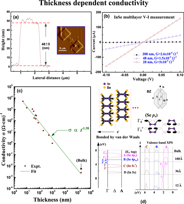
Figure 4. (a) FIB sample image and AFM measurement result of a multilayer InSe with thickness of 48 ± 5 nm available for conductivity measurement. (b) V-I measurement results of different thickness multilayer InSe samples. (c) Thickness-dependent conductivity of multilayer InSe measured from t ∼ 5 nm to t ∼ 180 μm. (d) Atomic arrangement, Brillouin zone, and EV-top electron configuration of the InSe are depicted in the upper part. The lower part reveals energy distribution of the valence-band states and representative XPS spectra of the layered InSe of different thicknesses [29].
Download figure:
Standard image High-resolution imageAs shown in figure 4(c), for the thickness-dependent conductivity of multilayer InSe, the σ changes from t ∼ 5 nm to t ∼ 180 μm is about six-order variation (103 to 10−3). It is inferred that six-order change in conductivity is mainly coming from the carrier concentration variation, but not largely handled by the carrier-mobility alteration. The increased carrier density of multilayer InSe with the thickness decreased from 180 μm to 5 nm may be still dominated by the relative enhancement in surface-to-volume ratio, wherein the layer plane of InSe may provide high surface density available for electrical conduction. The studied multilayer InSe is a p-type semiconductor and it will be verified in later MESFET V-I measurement. The p-type semiconductor behavior is caused by shallow-level defect state near the valence band edge (i.e. acceptor level Ea) to make hole emission from Ea. It is believed that the high hole concentration of the multilayer InSe with thickness decreased is not only caused by the increase of surface-to-volume ratio but also correlates with the valence-band structural change to render an increased carrier density in InSe with t < 10 nm. The inference was supported by previous x-ray photoelectron spectroscopy (XPS) study of some thin InSe films grown by van der Waals epitaxy [29]. The top part in figure 4(d) depicts the atomic arrangement of the monolayer InSe bonded by van der Waals force along c axis, hexagonal Brillouin zone (including symmetric points, Δ, A, Γ, M and K), and electronic states distribution of the Se 4pz at EV top of InSe. The left side in the lower part of figure 4(d) shows the representative electron density of states (DOS) along c direction (Δ symmetry) depicted from Γ point to A point. The EV top is the A band ( and
and  by Se 4pz). In energy order (deep into EV), they are B band (5−,6+ and 5+, 6− by Se 4pxy), C band (2−,3+ by antibonding In 5s*) and D band (In 5s). The right side in lower part of figure 4(d) is representative scheme for showing valence-band XPS spectra of the A, B, and C band when the thickness of the layered InSe is changed (derived from Ref. [29]). There are four different thickness of bulk, 100 Å, 36 Å, and 12 Å for the layered InSe being evaluated by XPS. For bulk and 100 Å samples, the DOS intensity of the A band in EV top is lower but broadened. For the thickness thinning out to 36 Å, the DOS counts in A band become higher intensity but separate into higher
  and lower
  states. For even thinner to 12 Å, the A band in the EV top is only consisted of
  but it shows the highest intensity of DOS to provide high conductivity (i.e. conjunction with high surface states and high surface-to-volume ratio to increase hole concentration). That is why a 5 nm multilayer InSe semiconductor in figure 3(c) even has a high conductivity reaching 5.1 × 10³ (Ω-cm)−1. As the thickness decreased from bulk, 100 Å, 36 Å, to 12 Å, the A band of layered InSe (see the representative XPS spectra in figure 4(d)) shifts lower into EV to enlarge the band gap while the DOS counts increased to promote the conductivity.
In order to evaluate electronic and optoelectronic properties of multilayer InSe device, a MESFET made by a ∼400 nm thick (area ∼0.01 mm2) indium selenide was implemented. The metal contacts of drain (D), source (S), and gate (G) were formed by Ag metal similar to the S-D condition of the PC measurement sample shown in figure 3(a). The inset in figure 5(a) depicts the representative scheme of the multilayer InSe MESFET operated at different gate voltage (VG) as well as various source-drain bias (VSD) conditions. The multilayer InSe was exfoliated and then transferred to mica as an insulating substrate. The silver electrodes were sputtered and patterned onto the the multilayer InSe. Figure 5(a) shows the voltage-current results of VSD versus ID under different VG values using the testing circuit as depicted in the inset. It is clear that the current values of ID in the gate voltage range of VG = −5 to −1 V show much higher current than those of VG = 1 to +5 V shown in figure 5(a). Under the operation condition of VSD > 0 V and VG varied from −5 to −1 V, the MESFET shows high ID current, which may be exactly a p-channel device coming from a p-type InSe. As shown in figure 5(a), each ID-VSD curve of different VG bias also reveals different cut-off voltage. This result displays general MESFET behavior of the multilayer InSe, which signifies scanning VSD will alter the threshold voltage from the gate in the InSe MESFET. Figure 5(b) depicts the V-I results of ID versus VG at different channel bias of VSD = 2, 1, 0, −1, −2, and −3 V, respectively. Essentially they show approximately parallel dependence at the negative VG values. Transconductance (gm) of a FET channel device can be defined as the change rate of ID versus VG at certain VDS condition given by:

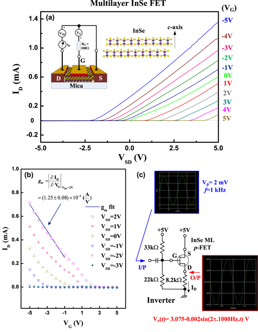
Figure 5. (a) ID-VSD measurement results of a multilayer InSe MESFET under different gate-voltage (VG) operations. (b) The ID-VG relation under different VSD bias. (c) Circuit design of an analog inverter by using the multilayer InSe MESFET. The testing result by using a sine wave as the input signal is also demonstrated.
Download figure:
Standard image High-resolution imageThe transconductance value of the p-channel multilayer InSe MESFET at VSD = 2 V can be calculated to be gm = (1.25 ± 0.08) × 10−4 (A/V) from the linear-fit slope shown in figure 5(b). To further use the multilayer InSe MESFET as an analog inverter a self-biased circuit design that containing two bias resistors of 22 kΩ and 33 kΩ as well as a drain resistor of 8.2 kΩ were implemented and demonstrated in figure 5(c). The power supply of the self-biased circuit was +5 V. A previously designed waveform generator & digital oscilloscope (i.e. personal-computer based instrument) was used as the signal's source as well as the output monitoring tool [30]. The input signal to the amplifier circuit is a sinusoidal wave with amplitude of Vp = 2 mV and frequency of f = 1 kHz and a coupled capacitor connects the input signal to the biased gate (G) (see figure 5(c)). The output is derived from a drain resistor (8.2 kΩ) and an inverted sine wave with the same amplitude and the same frequency as the input signal can be detected and observed in the monitoring tool (i.e. all the waveform images are shown in figure 5(c)). The testing result in figure 5(c) demonstrates well-behaved performance of the multilayer InSe MESFET of being an analog inverter.
The multilayer InSe MESFET has a direct-gap channel. A direct semiconductor based FET must show superior optoelectronics property to its optical behavior as a phototransistor. As shown in figures 1 to 3, the direct band gap (peak absorption energy) of multilayer InSe is about 1.24 eV (λ ∼ 1000 nm). To meet and show the best optoelectronic performance of the multilayer InSe, the multilayer MESFET in figure 5 was illuminated with a tungsten halogen to evaluate optically-enhanced transconductance gain for the MESFET (see the upper inset in figure 6(a)). The emission spectrum of the halogen lamp is close to the NIR region and its output power density was controlled to a weaker value of ∼0.5 mW · cm−2. Figure 6(a) shows the ID-VSD results of the multilayer InSe MESFET under the halogen lamp's illumination. In comparison with the dark condition in figure 5(a), with the same VG operation voltages, the ID current values in figure 6(a) obviously increased. It means an optically enhanced transconductance gain may occur in the FET device. The reason for increasing the transconductance gain can be explained from the lower inset of figure 6(a). When the p-channel layer of InSe was illuminated by the halogen lamp (white light), the photo-generated excess carriers (holes) will increase the current flow ID from S to D such as the representative scheme depicted in figure 3(c). This situation was similar to a previous nanosheet MoS2 FET, which possesses photo-induced current enhancement and thickness-modulated optical-gap change [31]. The threshold voltage in the nanosheet MoS2 photo-FET can be altered by the change in monolayers thickness [31]. As shown in figure 6, the photo-enhanced gm value of InSe MESFET calculated from figure 6(a) (at VSD = 2 V condition) is about (3.09 ± 0.22) × 10−4 (A/V), approximately three times larger than that of the dark condition. A self-biased phototransistor circuit by using the multilayer MESFET was also tested and demonstrated in figure 6(b). The same input signal as the dark condition in figure 5(a) was supplied to the circuit (i.e. sine wave with Vp = 2 mV and frequency of f = 1 kHz). The output signal was derived from the D terminal resistor (4.7 kΩ), and which coupled to the digital oscilloscope by an output capacitor. The digital-oscilloscope image in figure 6(b) clearly demonstrates an inverted sinusoidal wave expressed as V0(t) = −3 × 10⁻³ · sin(2π · 1000 Hz·t) V obtained from the output terminal of the phototransistor circuit. The testing result shows well-function performance of the multilayer InSe photo-MESFET device.

Figure 6. (a) ID-VSD results of the multilayer InSe MESFET (with different VG) under tungsten halogen lamp's illumination (P = 0.5 mW · cm−2). The representative scheme for showing the photo-generated carriers in the channel layer is depicted in the inset. The transconductance has increased to ∼3× in comparison with the dark condition. (b) The circuit design and signal testing result of the multilayer InSe phototransistor made on a mica substrate.
Download figure:
Standard image High-resolution image
4. Conclusion
In conclusion, we have firstly demonstrated thickness dependent conductivity of multilayer InSe with various thicknesses ranging from bulk to ∼5 nm. The conductivity of multilayer InSe reveals a decrease with the thickness increased from 5 nm to bulk following a relationship approximate σ ∝ t−1.38. The conductivity change with various layer thickness is owing to the variation of surface-to-volume ratio, surface-state effect, and density-of-states variation (i.e. t < 10 nm) in the valence band of the multilayer InSe. To verify and identify the structural and band-edge characteristics of the multilayer InSe, μ-PL & μ-Raman spectrum is simultaneously taken. The hexagonal layered structure of multilayer InSe can be verified and a peak emission wavelength of ∼1000 nm is detected. Temperature-dependent PzR measurements determine an accurate temperature-energy shift relation of direct band gap for a multilayer InSe device operated at a higher temperature above 300 K. The peak photoconductive responsivity of a CVT-grown multilayer InSe photoconductor is ∼7.3 A W−1. The energy position is close to the direct band edge of InSe approaching 1000 nm (∼1.24 eV). Based on the multilayer InSe photoconductor (with source and drain) together with forming an additional Ag metal gate, a multilayer InSe MESFET with a p-conduction channel has been implemented. A transconductance gain of gm = (1.25 ± 0.08) × 10−4 (A/V) has been obtained. Under the illumination of a tungsten halogen lamp with weak power density of P ∼ 0.5 mW · cm−2, the multilayer InSe MESFET demonstrates three times enhancement in the phototransconductance gain as comparing to that of the dark condition. Circuit design of an analog inverter & amplifier has verified and exhibited the well-behaved function of the multilayer InSe photo-MESFET device.
Acknowledgments
This work was sponsored by the financial support from the Ministry of Science and Technology of Taiwan under the grant No. MOST 104-2112-M-011-002-MY3. It is thankful to Y J Chu and Y H Chen for their technical assistance.