

Abstract
Borophene, a two-dimensional monolayer of boron atoms, was recently synthesized experimentally and was shown to exhibit polymorphism. In its closed-packed triangular form, borophene is expected to exhibit anisotropic metallic character with relatively high electron velocities. At the same time, very low optical conductivities in the infrared-visible light region were predicted. Based on its promising electronic transport properties and its high transparency, borophene could become a genuine lego piece in the 2D materials assembling game known as the van der Waals heterocrystal approach. However, borophene is naturally degraded in ambient conditions and it is therefore important to assess the mechanisms and the effects of oxidation on borophene monolayers. Optical and electronic properties of pristine and oxidized borophene are here investigated by first-principles approaches. The transparent and conductive properties of borophene are elucidated by analyzing the electronic structure and its interplay with light. Optical response of borophene is found to be strongly affected by oxidation, suggesting that optical measurements can serve as an efficient probe for borophene surface contamination.
Export citation and abstract BibTeX RIS
1. Introduction
Borophene is known to be polymorphic [1], thus the word borophene denotes generically various two-dimensional (2D) monolayers of boron (B) that have been discussed previously in the literature [2–6]. Many of these B monolayers contain hexagonal holes  stabilizing the planar structure. The fundamental ground state according to [2] is obtained for hexagonal hole concentration x = 0.1–0.15 in
  is thus the densest boron limit, which corresponds to the closed-packed triangular borophene. In dense B monolayers cases, the buckling and the coupling between sublattices has been shown to enhance their energetic stability and possibly rise to the emergence of distorted Dirac cone [3]. Magnetic properties have also been predicted for one of these B monolayers [7].
At least two experimental works reported recently the synthesis of borophene monolayers via controlled atomic deposition of boron atoms on a silver (Ag) surface [8, 9]. Various phases were observed, depending mainly on the deposition rate and the temperature, attesting the predicted large polymorphism of borophene. In the following, we focus on one of these phases and thus refer to borophene solely as the dense buckled monolayer of B atoms arranged in two inter-penetrating rectangular sublattices (or equivalently the buckled triangular lattice), i.e.  , which was presumably one of the phases recently synthesized [8].
The reported phonon band structure of the free standing borophene attests small instabilities [6, 8, 10, 11]. Such instabilities seem to be further washed out when borophene is fully hydrogenated, i.e. forming borophane, for which the emergence of a Dirac cone was recently predicted [12]. Applying strain to borophene can also wash out the phonon instability. These results suggest that the underlying Ag surface could stabilize borophene in the experiments. When decoupled from the substrate, such borophene flakes may either stay trapped in its local metastable minimum or undergo a phase transition to a lower energy phase.
Free-standing borophene displays attractive properties. It is metallic while its bulk phases are semiconducting. It exhibits a highly anisotropic metallic character due to its anisotropic atomic structure [8, 10], similarly to phosphorene [13], although phosphorene is a ∼2 eV band gap semiconductor. In contrast to graphene, high optical transparency (nearly 100% transmission) is predicted up to roughly 3 eV. Combining the good metallicity with such a high optical transparency could make borophene a good candidate as a transparent conductive 2D material with possible applications in photovoltaics and touch screens. Borophene is also predicted to have interesting mechanical properties. It is found to be a hard and brittle 2D material with anisotropic critical strains and negative out-of-plane Poisson's ratio [14, 15]. Finally, combining its promising properties with the ones of other 2D materials such as graphene or transition metal dichalcogenides, might lead to new van der Waals heterostructures with superior properties.
However, chemical stability of borophene with respect to ambient conditions, and in particular with respect to oxygen (O) has not been discussed so far. This is an important issue to consider since signature of oxidation was already reported in the pioneer experiment of Mannix et al [8]. How the electronic and optical properties of pristine borophene change as a consequence of such a surface degradation? In the present paper, one answers this question using a first-principles approach. Different adsorption sites for oxygen atoms are considered and the calculated adsorption energies demonstrate indeed that borophene is prone to chemically adsorption. The electronic structure remains metallic upon oxygenation but the decrease of electronic dispersion and the defect induced-disorder is expected to lower the conductivity. Furthermore, optical conductivities are found to increase with oxidation which lower the optical transparency, suggesting a high optical sensitivity of borophene with respect to any surface modifications, especially in the infrared region.
2. Methods
First-principles simulations were conducted to relax stresses, optimize atomic positions, to compute electronic band structures, density of states (DOSs), optical conductivity, transmittance and reflectance of pristine and oxidized 2D borophene sheets. Calculations were performed using the self-consistent density functional theory (DFT) method as implemented in the SIESTA [16] package. The exchange-correlation energy and electron–ion interaction are described using GGA-PBE [17] functional and norm-conserving pseudopotentials [18] in the fully non-local form. A double-ζ polarized basis set of numerical atomic orbitals is used and the energy cutoff for real-space mesh is set to 500 Ry. The energy levels were populated following a Fermi–Dirac distribution function with an electronic temperature of 300 K. The geometries were relaxed until the forces on each atom and the stress on the unit cell were less than 0.01 eV Å−1 and 0.001 GPa, respectively. An inter-layer vacuum distance ≈ 30 Å was used in order to avoid any spurious image interaction. Spin polarization has been accounted for in all calculations but none of them exhibited a net magnetic moment. A fine k-point grid of 100 × 100 × 1 for the unit cell and an equivalent one for the n × n supercell was employed using the Monkhorst–Pack scheme [19]. A denser k-point grid of 900 × 900 × 1 was used to evaluate the DOS and the average velocity was computed using central numerical derivative as

where  are the k-points sampling the Brillouin zone, b is the band index, and
  is a delta-Dirac function centered on each of the eigenvalues and approximated by a Lorentzian in the numerical computation. Beyond DFT calculations were performed on pristine borophene to include self-energy corrections to the eigenvalues through a G0W0 approach on top of a LDA starting point as implemented in the ABINIT package [20–22].
The optical properties were computed from the imaginary part ( ) and real part (
 ) of the complex dielectric function (ε). The Kramers–Kronig relation was employed to obtain
  from
from  and since borophene is a metal, a Drude term was added to both part of ε as

with  where
where  is the plasmon frequency and
  where τ is a relaxation time in the Drude model. The parameter Γ was varied from 20 Ha (≈ 544 eV) to 0.2 mHa (≈ 5.44 meV) which corresponds to τ varying from 1.21 × 10⁻¹⁸ s to 1.21 × 10⁻¹³ s, respectively. For optical properties, the integration over the Brillouin zone was performed on a dense k-point grid of 1100 × 1100 × 1 in case of the unit cell (an equivalent grid was used for the case of supercells), taking into account all the available electronic bands for interband transitions, and a broadening factor of 25 meV was applied. To account for the 2D nature of the system, the imaginary part of the dielectric function ε was renormalized [23] (including both interband transition and Drude terms), as

where H is the total height of the 3D periodic simulation cell (in our case 30 Å), and h is the polarizable electronic thickness which was estimated using the buckling height and the van der Waals atomic radius [24] ( = 4.73 Å and
  =3.40 Å).
3. Electronic structure
3.1. Pristine borophene
The lattice parameters of the optimized rectangular unit cell of borophene are displayed in figures 1(a)–(c), i.e. (a = 1.6212; b = 2.8699) Å with a buckling height of 0.89 Å between bottom and top atoms (B1 and B2 respectively). The calculated cohesive energy ( ) is −6.707 eV/atom (see equation (5)) while the cohesive energy of the bulk crystal of boron (α-rhombohedral with 12 B atoms per unit cell) is −7.262 eV/atom, i.e. borophene is metastable by 0.555 eV/atom with respect to bulk phase.

where  and
and  are the total energies of an isolated B atom and of the borophene layer containing
  boron atoms. Other boron monolayer structures have been reported with differences in total energies with respect to bulk phase being in the order 0.32–0.40 eV/atom [2, 3]. This means that the present borophene structure (buckled closed-packed triangular) is not the most stable 2D phase but may be favored by the underlying Ag surface on which it is grown.

Figure 1. (a) and (b) side views, (c) top view, of a 3 × 3 borophene supercell. The central 1 × 1 unit cell contains two boron atoms (B1 and B2 depicted as green and blue spheres, respectively) and is delimited by red filled lines while the repeated cells are delimited by red dashed lines. (d) Electronic band structure and density of states (DOS) with zero energy aligned to the Fermi level (EF). The Brillouin zone is shown in the inset. The highest group velocity (6.63 105 m s−1) for a band crossing the Fermi level is highlighted by a red dashed line. (e) 3D plot of the two electronic bands (only for positive ky) crossing the Fermi level (symbolized by the semi-transparent plane) in an energy window ∼ [−1;+1] eV. (f) Comparison between Khon–Sham (KS) band structures with Siesta (GGA-PBE) and Abinit (LDA) with the G0W0 corrected one.
Download figure:
Standard image High-resolution imageThe electronic band structure (figure 1(d)) exhibits a priori a strongly anisotropic metallic character as the bands are found to be highly dispersive in the kx direction (Γ–X and Y–S) with relatively high group velocity of 6.6 105 m s−1, while it appears that no bands cross the Fermi level in the ky direction (Γ–Y and X–S) as reported previously [8, 10]. Notwithstanding, one also notes that dispersion occurs along the oblique Γ–S path. This reveals that bands can actually cross the Fermi level parallel to the ky direction in some region of the 2D Brillouin zone. In order to have better insight on the exact anisotropy of the electronic structure it is thus important to plot the electronic band structure in the whole 2D Brillouin zone and identify the Fermi surface (which in 2D actually reduces into a Fermi line) (see figure 1(e)). While electronic bands always cross the Fermi level for any line parallel to kx, this is not the case for lines parallel to ky. Therefore, it is expected that transport will occur only for selective wave vectors k whose kx component belongs to the allowed region (figure 1(e)). This sets a maximal angle (k ) for the wave vectors k = (kx, ky) ≡ (kr, k
 ). One also notes, that the two bands crossing the Fermi level become exactly degenerate at the edge of the Brillouin zone along the S–Y path.
Then, the DOS around the Fermi level (figure 1(d)) exhibits an almost planar shape, typical of 2D free electron gas, except when approaching an energy equal to EF−1 eV, where a van Hove singularity is observed. This energy point corresponds to a saddle point of an electronic band at the Γ point (figures 1(d) and (e)). The presence of this peak generates a native asymmetry between electrons and holes which will add to the above mentioned asymmetry between transport directions. Finally, the band structure of borophene was recalculated within a LDA approach using ABINIT package and then corrected by applying a one shot G0W0 approximation to the quasi particle problem. No significant changes were observed between the Kohn–Sham structure and the G0W0 one. One can only notice an increase of the local band gap at the Γ point, and generally speaking an increase of the Fermi velocity.
3.2. Oxidized borophene
Experimental measurements indicate that bare borophene on a Ag substrate is partially oxidized within several hours unless it is capped with amorphous silicon/silicon oxide [8]. Even after encapsulation and after several weeks, residual oxygen bound to borophene has been found [8]. Therefore, the effect of oxygen on the electronic and optical properties of borophene cannot be ignored and should be addressed. Due to computational limitations, however, one-side oxidation of the free standing borophene is considered rather than the surface oxidation of the full borophene-substrate system. It is worth noting that the detached free standing borophene can experience strong structural changes before the oxidation takes place, due to the aforementioned small phonon instabilities. Nevertheless, our simulations aim to describe the properties of oxidation of the supported borophene albeit with the assumption of a limited impact of the underneath substrate.
A 3 × 3 borophene supercell is first considered with four adsorption sites which correspond to a position on top of a boron atom (B1 or B2), a bridge position either in between first nearest-neighbor atoms (along the x-direction) or in between third nearest neighbor atoms (along the y-direction) of the top layer (B2–B2) (see supplementary figure 7). The last case is found to be the most stable adsorption site with a relatively high adsorption energy of −4.548 eV. The adsorption energy of the other configurations can be in found in supplementary table 1. The adsorption energy ( ) has been computed with respect to total energies of isolated borophene and molecular oxygen (O2) as
A negative value of  means that the adsorption is favorable.
During the adsorption, the two B2 atoms bound to the O atom are slightly displaced out of the top layer and get closer to each other as depicted in figures 2(a)–(c). The corresponding folded electronic band structure (compared to the band structure of pristine borophene), as well as the DOS and the average velocities (vx and vy), are plotted in figure 2(d). From the band structure, one notes that many band crossings and band degeneracies are avoided and lifted up, respectively, but it remains difficult to clearly assess the impact of oxygen adatom because of the folding. However, the impact on the DOS is more obvious. Several new peaks appear and are well distributed in energy which makes the DOS curve much more noisy than in pristine case but still non-zero at the Fermi level (no gap opening). The band structures and DOS for the other adsorption sites are displayed in supplementary figure 8. Even more obvious than the impact on the DOS is the impact on velocities. Indeed, as it can be seen in figure 2(d), right to the DOS, the computed average velocity along the x- and y-direction largely decreases when the O adatom is incorporated compared to the pristine case. One also notes that the anisotropy has almost disappeared. Finally, charge transfer between borophene and O adatom has been investigated using Voronoi and Hirshfeld methods. The O adatom is found to loose 0.15–0.17  in bridge positions while it looses 0.23–0.25
  in top positions. The electronic charge gained by borophene is spread over the system.
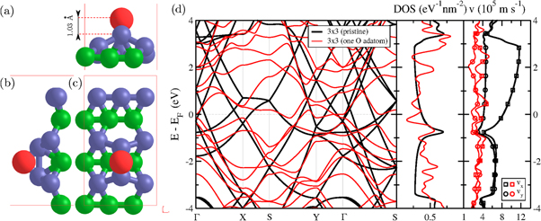
Figure 2. (a) and (b) side views, (c) top view, of a 3 × 3 supercell of oxidized borophene. Boron atoms B1 and B2 are depicted as green and blue spheres respectively while the oxygen adatom O is represented by a red sphere. (d) Electronic band structure and density of states (DOS) with zero energy aligned to the Fermi level (EF).
Download figure:
Standard image High-resolution imageTo provide a better understanding of the modifications induced by O adatoms, it is also essential to investigate its dependence as a function of the concentration. For this purpose, in addition to the previous 3 × 3 supercell, larger supercells have been considered i.e. a 4 × 4, a 5 × 5, and a 6 × 6 (supplementary figure 9). The corresponding oxygen surface density are n =
=  ,
,  ,
,  , and
, and  cm−2. The dependence on the DOS is illustrated in figure 3. As it can be seen, the DOS remains always non-zero and thus the oxidation preserves a priori the metallic character. However, due to the presence of numerous DOS peaks and the velocity decreasing one can anticipate the presence of localized states around the defects and thus strong scattering mechanisms which should largely degrade the electronic conductivity and mobility in oxidized borophene.
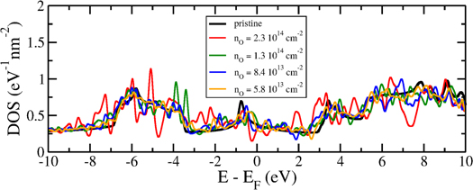
Figure 3. Electronic density of states for different concentrations of oxygen adatoms (nO).
Download figure:
Standard image High-resolution image4. Optical properties
4.1. Pristine borophene
Beside its potentially interesting anisotropic conduction properties, pristine borophene is expected to be highly transparent owing to its extremely small thickness. This could make the material interesting for photovoltaic applications and touch screens. A transparent conductor is a priori a counter-intuitive property since common bulk metals are usually not transparent but instead looks gray and shiny to human eyes. It is because a large part of light is reflected at the interface. It is however well known that beyond the plasmon frequency, i.e. for photon energy larger than  , the reflectance can strongly decrease and possibly render the metal transparent. For most of metals the plasmon frequency is in the ultra-violet (UV) which means they indeed reflect light in the visible region. However, when the thickness is reduced to few (or even one) atomic layers (the so-called thin film limit; TFL), the reflectance drops to nearly zero and the transmission increases to almost 100% and their variations are actually mostly related to the optical conductivity. In the following one assesses carefully the optical properties of borophene accounting correctly for the 2D nature, in contrast to a recent work [10] where the 3D bulk formula was considered, showing relatively high reflectance. We first discuss the optical conductivity and second the transmittance (the reflectance plots can be found in supplementary material).
The real part of optical conductivity ( , where
  is the vacuum dielectric constant) of borophene is first investigated and is displayed in figures 4(a)–(d). Different polarizations of light are considered, i.e. an electric field along the x direction, along the y direction, and average of both directions (i.e. a light propagating along the z direction). In figure 4(a), the scattering time parameter originating from the Drude model is fixed to τ = 1.21 10−18 s (Γ = 20 Ha) which is a very small value describing thus a 'bad' metal (actually a mean free path in the order of a picometer). At the same time one can see, from equations (2) and (3), that for such a large value of Γ, the Drude contributions (
 ) becomes negligible, just as if one was using only the usual interband transitions to describe the optical properties. In such a situation, the optical conductivity is found to be almost zero for low energy radiation up to 3 eV (i.e. violet, close to the end of visible light). Then in the UV part, the optical conductivity increases slowly up to 6.5 eV before exhibiting an enhanced signal composed of a series of four peaks at 6.5, 8.2, 8.5 and 9.6 eV. The low optical absorption of borophene is even better highlighted by comparing it with the one of monolayer graphene (gray dashed lines in figure 4) whose optical conductivity is between 1 and 2
  (with
(with  ) up to 3 eV. The fact that borophene appears to be transparent in the infrared-visible region is related here to the fact that it has been considered as a bad metal (and acts thus as an insulator) and that interband transitions occur only above 3 eV. One also notes the anisotropy of the optical absorption between x and y directions. In particular, the optical conductivity remains very small up to 6.5 eV for polarization along the x direction.
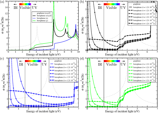
Figure 4. (a) Comparison of the optical conductivity of pristine borophene with pristine graphene. Different electric field orientations are considered, i.e. (1,0,0) (x), (0,1,0) (y), and (1,1,0) (x + y)/2. (optical conductivity of graphene being isotropic only the (1,1,0) case is plotted) (scattering time parameter of the Drude model τ = 1.21 × 10⁻¹⁸ s). (b)–(d) Zoom in the low energy energy region of borophene optical conductivity for different values of the scattering time parameter of the Drude model. (b)–(d) correspond to (1,1,0), (1,0,0), and (0,1,0) electric fields respectively.
Download figure:
Standard image High-resolution imageWhen going now to the case of a 'good' metal, that is increasing τ up to 1.21 10−13 s (mean free path in the order of 102 nm) (figures 4(b)–(d)), one observes first an almost constant increase of the optical conductivity forming a plateau, and then a divergence at low energy going towards a delta-Dirac function at zero energy which finally restores a very low optical conductivity in the visible region, i.e. similar to the one observed in figure 4(a) except for the zero energy limit. This is the expected behavior for  of a perfect metal in the Drude model, i.e. a delta-Dirac function at zero energy. This reflects the fact that in the static limit, i.e. for a constant electric field, the dc conductivity tends to infinity (
 ) as the scattering vanishes and hence does not damp the acceleration of electrons caused by the electric field. For an alternating field the real part of the ac conductivity is zero (
 ), and the ac conductivity becomes actually purely imaginary (
 ). Hence, in both limits of a bad and good metal, borophene would exhibit nearly zero conductivity in the visible region. As mentioned previously, the fact that the optical conductivity is zero in the visible region implies, following the TFL, that the transmittance goes to 100% and that the material should be fully transparent.
The actual transmittance and reflectance have been computed following both rigorous Fresnel equations, and TFL equations (that are obtained from the former ones by taking the limit of small thickness). In contrast to the bulk case where reflectance accounts only for one interface (typically between vacuum and the material), the reflectance in thin films accounts for the presence of a back side interface which produces secondary reflections. As most ab initio codes do not have this particular treatment for 2D thin systems, it is important to carefully compute optical properties using general Fresnel equations or at least TFL equations. Although small differences are observed in reflectance curves, both approaches yield very similar results for transmittance validating therefore the TFL in case of graphene and borophene. The reflectance (R), the transmittance (T), and the absorbance (A), in TFL are given by [25, 26]


where  is the complex refractive index for a non-magnetic material. The superindex indicates which medium it refers to, i.e. the medium above the film from where light comes, the medium below the film into which light is transmitted, and the film itself. Equations (8), (10) and (12) give the reduced expression of equations (7), (9) and (11) respectively, when above and below media are vacuum.
  , where
  is the film thickness (or equivalently the polarizable electronic thickness defined as h in method section). (The fully rigorous Fresnel equations are also given in supplementary material, but as mentioned both sets of equations gives similar results.) The transmittance of borophene is displayed in figure 5. The scattering time parameter is first fixed to τ = 1.21 10−18 s (bad metal case) in figure 5(a) for which one observes high transparency up to 6 eV, and a complete transparency (100% transmission) up to 3 eV. High anisotropy is also found between light polarization with respect to crystal orientation. Then in figures 5(b)–(d) corresponding to these different polarization of the electric field, one varies τ up to 1.21 × 10⁻¹³ s (good metal case). In the visible range, T starts to decrease forming a plateau at 96%–98%, and then increase again to 100%. In the infrared range, T is first strongly reduced especially close to zero energy where T eventually drops to zero in a very good metal case. The reflectance curves can be found in supplementary figure 10 and corroborate results found for optical conductivities and transmittance. The reflectance is nearly zero in the infrared-visible range except when considering Drude model with long scattering time (τ = 1.21 × 10⁻¹³ s) especially in the infrared region.
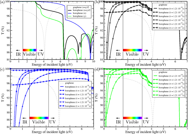
Figure 5. (a) Comparison of the transmittance of pristine borophene with pristine graphene. Different electric field orientations are considered, i.e. (1,0,0) (x), (0,1,0) (y), and (1,1,0) (x + y)/2. (Optical conductivity of graphene being isotropic only the (1,1,0) case is plotted.) (Scattering time parameter of the Drude model τ = 1.21 10−18 s.) (b)–(d) Zoom in the low energy energy region of borophene optical transmittance for different values of the scattering time parameter of the Drude model. (b)–(d) Correspond to (1,1,0), (1,0,0), and (0,1,0) electric fields respectively.
Download figure:
Standard image High-resolution image4.2. Oxidized borophene
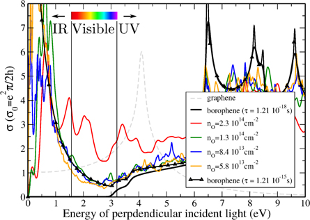
The optical conductivities of oxidized borophene systems are presented in figure 6 and correspond to the 3 × 3, 4 × 4, 5 × 5, and 6 × 6 supercells (depicted in supplementary figure 9). At low energy, prominent peaks are clearly observed in the infrared (IR) spectrum part. Optical conductivity is also significantly increased in the visible light region. Except for the 3 × 3 supercell, the optical conductivity curves of the larger oxidized borophene supercells are nicely reproduced using pristine borophene and a Drude term with τ = 1.21 × 10⁻¹⁵ s. Such a large increase in the infrared suggests that optical conductivity is highly sensitive to probably any surface modification, which makes optical conductivity/absorption measurement an interesting tool to investigate the cleanness of borophene surface. This result also implies that transparency of borophene will be slightly limited by surface chemical functionalization, although the absolute values in figure 6 indicate that even for reasonably high degree of oxygenation (1013 cm n
n cm−2), the optical conductivity in the visible range is lower than in pristine graphene.
Figure 6. Optical conductivity of pristine and oxidized borophene as well as pristine graphene for comparison.
Download figure:
Standard image High-resolution image
5. Conclusion
Electronic and optical properties of pristine and oxidized borophene have been extensively studied using a first-principles approach. Pristine borophene is found to be metallic with a relatively high electronic velocity (6.6 105 m s−1). The full anisotropy of its electronic structure has been revealed by inspecting carefully the Fermi surface (line) in the 2D first Brillouin zone showing that the permitted wave vectors at the Fermi energy have a maximal angle. Pristine borophene has also been found to exhibit extremely low optical conductivities due to the absence of interband transitions up to 3 eV. Anisotropy was also reported for the computed optical conductivity showing that for an electric field oriented along the main conductive direction (x-axis, that is along non-buckled B lines), the material stays optically inactive up to 6.5 eV. Although the exact value depends on disorder (through the scattering time τ), the calculated transmittances have been shown to possibly reach 100% in the visible range making borophene more transparent than graphene. Then, it has been predicted that oxidation of borophene is highly probable due to the reported high adsorption energies (E 4.0–4.5 eV). Different adsorption sites were considered and the preferred one was found to be in between adjacent B lines. Upon oxidation, borophene remains metallic. However, from the computed electronic structure one anticipates dc conductivity degradation due to the disorder which increases the effective masses and decreases velocities. Finally, optical properties of oxidized borophene display a large increase of the optical conductivity and reflectance in the infrared region while it remains relatively low (smaller than in pristine graphene) in the visible region for reasonable degree of oxygenation, letting the opportunity to investigate borophene as a candidate for transparent conductive material.
Acknowledgments
AL, ARBM and J-CC acknowledge financial support from the Fédération Wallonie-Bruxelles through the Action de Recherche Concertée (ARC) on 3D nanoarchitecturing of 2D crystals (no. 16/21-077), and from the Belgium FNRS. This project has received funding from the European Union's Horizon 2020 research and innovation programme under grant agreement No 696656. Computational resources have been provided by the supercomputing facilities of the Université catholique de Louvain (CISM/UCL) and the Consortium des Équipements de Calcul Intensif en Fédération Wallonie Bruxelles (CÉCI) funded by the Fonds de la Recherche Scientifique de Belgique under the convention N° 2.5020.11.