Abstract
Novel 2 × 2 mm2 MEMS capacitive plates with two cavities (two capacitors) have been designed, modeled and fabricated for power harvesting by utilizing residual mechanical vibration in the environment using the electrostatic mechanism. The device is unique in the use of an innovative two-cavity design and electroplated nickel as the main structural material. When the capacitance increases for one capacitor, it will decrease for the other. This allows us to use both up and down directions to generate energy. The two-cavity design has achieved higher average power than conventional single-cavity devices under a wide range of vibration frequencies and amplitudes based on the time-domain simulations using Matlab. The movable plate was designed to vibrate without deformation and with resonance frequencies of around 900 Hz and lower using COMSOL finite element tool. The prototype two-cavity MEMS variable capacitor has been successfully fabricated using surface micromachining. The initial testing to investigate the electrical dynamic behavior and power generation from the fabricated devices was also implemented.
Export citation and abstract BibTeX RIS
1. Introduction
Power harvesting from residual unwanted mechanical vibration is of engineering interest. For example, cabling will be greatly simplified if the autonomous sensors can be powered by the structure vibration in an aircraft or automobile. Similar simplification is also achieved in outdoor structures such as bridges and cellular towers. Recently, vibration and motion have been investigated as a source for energy scavenging using inertial devices which convert environmental vibration into electrical power by moving a proof mass suspended within a frame. The devices use one of three transduction mechanisms: electromagnetic [1–3], piezoelectric [4–7] and electrostatic [8–12]. Yeatman and colleagues performed extensive calculations and compared the normalized power of many inertial energy scavengers reported in many works of literature. They found that the power results do not show clear differences between the three transducer types in terms of normalized power [13, 14].
The electromagnetic approach mainly uses large devices that employ a magnet moving through a coil or a coil on the proof mass moving through the magnetic flux from the permanent magnet [11, 15]. It is difficult for these devices to achieve sufficient forces for low-frequency applications. The micromachined devices tend to result in low output voltages making rectification difficult due to the limited number of coil turns [16]. Piezoelectric devices effectively produce output even at low frequencies, and generally at reasonably high voltage levels. Implementation requires a piezoelectric material, usually a ceramic such as PZT in a monolith or thin film form. The latter can be incorporated into a MEMS device. These devices are most suited to resonant devices due to their small damping force. Moreover, the output impedance of the piezo element is dominated by its capacitance, which due to its small size cannot be turned out with a realistic inductance at the frequencies of interest [16]. We have chosen to work with an electrostatic mechanism because it is CMOS compatible which allows the integration of electronic circuits and MEMS parts on the same chip. This integration will lead to the production of low-cost arrays of energy sources. The approaches of electrostatic capacitive plates with various designs have been studied in many research works in the past. These include a multi-gap comb fingers microstructure [17, 18] and suspended proof mass within a frame above the substrate [19] for energy scavenging and voltage step-up conversion. Most of the reported energy sources use bulk micromachining in which the proof mass can be formed from the whole thickness of the wafer [20]. Electrostatic devices that take advantage of using electret material were recently reported [21–23]. Their devices achieved bi-directional power generation from in plane motion using a silicon comb drive microstructure. Suzuki reported a maximum power generation of 0.56 µW and a high surface charge density of 1.5 mC m−2 using devices with a dimension of 10 mm [23]. It should be pointed out that high-quality electret materials with long-term stability might be achieved. We intend to use electret material in our devices in future processes. To our knowledge, no one has attempted to design or fabricate two-cavity MEMS parallel plate variable capacitors for bi-directional power generation from out-of-plane motion.
In this paper, the design, operational principle, time-domain simulation and finite element modeling of two-cavity MEMS variable capacitors are presented. The fabrication processes have been developed and optimized for building these devices. Initial characterizations have been implemented to confirm the successful suspension of the movable plate and investigate the dynamic response of the device before bonding the second cavity. The dynamic response and output power generation testing were performed through biasing the device with an external dc voltage source.
2. Design and principle of operation
The MEMS variable capacitors are designed with two capacitive cavities connected in series (see figure 1). When the capacitance increases for the bottom cavity, it will decrease for the top cavity. This allows us to use the two capacitive cavities to optimize the efficiency of power harvesting. In addition, the energy is generated in both directions of motion of the movable plate, which increases the energy harvesting. In the case of step-up voltage conversion, the top electrode can be used as an actuator which permits the decrease of the off-capacitance and hence increases the capacitor ratio.

Figure 1. The imaging 3D view of 2 × 2 mm2 MEMS variable capacitors' geometries: (a) a single device without the second capacitive cavity, (b) an array of four devices with the top silicon plate and two capacitive cavities.
Download figure:
Standard imageThe device consists of a movable thick plate (proof mass) with an area of 2 × 2 mm2 sandwiched between two fixed plates, two air cavities, four suspension beams with a serpentine shape which are connected to the address lines on a silicon substrate via four anchors, four tabs for wafer bonding and two layers of silicon oxide/silicon nitride (SiO2/ Si3N4) dielectrics to enhance the dielectric property of the capacitors and to insulate the Au stoppers. In future work, the SiO2/ Si3N4 layer will be used to provide the polarization voltage. Charges that are injected into the electret layer are trapped at the interface between the two dielectric layers [24]. The movable plate, suspension beams, anchors and four tabs are created using nickel electroplating source which is a mechanically durable material with controllable residual stress. After fabricating and suspending the movable plate on one silicon substrate, the second air cavity is created by bonding a second silicon substrate onto the first one. The second substrate contains patterned Cr/Au electrodes and SiO2/Si3N4 layer, and electroplated indium tabs for wafer bonding. The indium tabs are aligned with the Ni tabs on the first substrate and bonded together at relatively low temperature to form the second air cavity.
An ideal charge control strategy of the MEMS capacitive plates is uniquely suitable for power harvesting applications using two capacitive cavities as follows: two capacitive cavities are initially charged by a low dc voltage source, when the gap of bottom cavity starts decreasing, the capacitance increases and causes the bottom cavity to take in more charge [25, 26]. When charging stops at the lowest bottom position, the movable plate tries to bounce back to a higher position so that the gap of bottom cavity increases and the gap of the top cavity decreases. The capacitance decreases and the voltage increases because the total charge is conserved in the bottom cavity. Discharge of the bottom cavity starts when the voltage reaches a preset higher value. At the same time, the gap decrease and capacitance increase cause the top cavity to take more charge. Discharge of the top cavity starts when the movable plate moves back to the lowest bottom position with a higher voltage. The above sequence repeats to achieve continuous power generation utilizing the two interactive outputs from both top and bottom cavities.
3. Modeling
3.1. Time-domain simulation
The first time-domain model was created based on the conventional design of electrostatic power scavenger with a single cavity. The movable plate is supported by four serpentine springs. Four stoppers are placed on the fixed plate (figure 2) to avoid short circuit during the collision of the movable plate with the fixed one. The schematic of electrical control is shown in figure 2. Output battery voltage is higher than that of the input power source. Charge across the plates is controlled by diodes. The whole arrangement is placed on a base to which vibration force is applied.
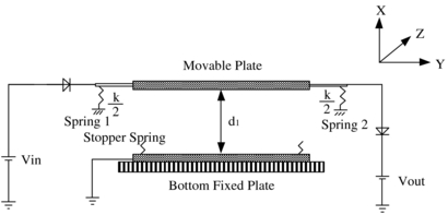
Figure 2. The schematic of the arrangement of springs and electrical control circuit for modeling conventional single-cavity power scavenger.
Download figure:
Standard imageWe assume that the package containing the capacitor is subjected to sinusoidal displacement given by (1) and the nonlinear equation of motion for the movable plate is given by (2):


where d1 is the gap between the two plates, m is the mass of the movable plate and k is the stiffness of the elastic supports. The coefficient c accounts for the damping, mainly from the squeezed air film in the gap of the capacitor. The term fi given by (3) represents the inertia force if the device is subjected to base excitation. The term fe refers to the electrostatic force over two capacitive plates due to electric charge stored between the plates. Through charging and discharging, the capacitive plates exchange energy with the electrical components both upstream and downstream, mechanical energy is dispensed in the process. If the device is sealed in a vacuum, the mechanical damping can be negligible. The capacitance of the device with a single air cavity is given by (4):

where ε is the electric permittivity, A is the plate area and d is the distance of the gap. For plates with a varying gap, the electrostatic force caused by a voltage difference is given by (5):

Since the gap is varying, this force is dependent on the plate displacement. When the gap decreases, the electrostatic force increases. This force is nonlinear which means that the increase is not proportional to the displacement. The increase in the electrostatic force may overwhelm the restoring force of the elastic supports to cause the gap to collapse. When this is caused by the gradual increase of the voltage, a critical voltage, called the pull-down voltage, is known to exist as

where d0 and C0 are the gap and capacitance at static equilibrium when no voltage is applied. The electrostatic force is determined by the voltage on the capacitor. The voltage is calculated from the charge on the plate given by

The charge on the plate can be determined by keeping track of the current flowing in and out of the capacitor. However, since the plate capacitance is very small, charging time and discharging time are very short. Keeping track of the current flow would require an additional differential equation. The numerical solution of this additional equation would require extremely small integration time steps to prevent numerical instability. Since the short charging and discharging time can be ignored, we assume that the charge on the plate is constant when no charging or discharging takes place. That is, Q is constant if Vin < Vc < Vout. By ignoring the charging and discharging time, we set up the following limitations on the voltages on the capacitor: minimum Vc = Vin and maximum Vc = Vout. The above limitations are imposed at the end of each time integration step. If the voltage exceeds Vout, we calculate the excess electric charge which is moved to the battery Vout. If the voltage is below Vin, Vc is reset to Vin.
To avoid collision between the plates, we placed four stoppers on the fixed plate. The moving plate makes contact with the stoppers when its displacement is 80% of the initial gap. The stopper is modeled as a very stiff spring whose spring constant is 1000 times the plate suspension. Therefore, the stopper acts like a nonlinear spring and its force can be written as

The damping coefficient c represents the loss of energy associated with the plate motion. The damping by the air surrounding the plate is the main contributor to the damping. We introduce the damping ratio ζ given by (9), and introduce the dimensionless displacement: d1 = d0 (1+x). We obtain the nonlinear equation of motion given by (10):


For the single-cavity model, the movable plate will move up and down and after some time it will start striking on a stopper spring at the bottom only. It does not have any limit in the upward direction. For the vibration with low forcing frequency and amplitude, the movable plate will stick to the bottom plate's stopper because of the pull-down effect and then stays there which results in no stepping up of voltage. Using the equations of forces acting on the movable plate we developed the Matlab program to simulate the one-cavity system.
The model of the MEMS capacitive plates with two cavities was similarly established which consists of two variable capacitors with gap 1 and gap 2. Input and output dc voltage batteries are connected to the fixed plates, and the movable plate is grounded (see figure 3). Charge across the plates is controlled by diodes.
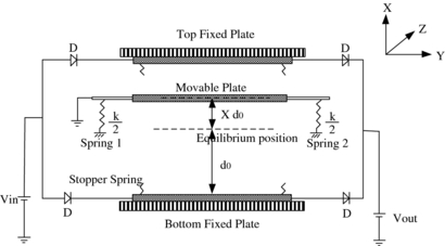
Figure 3. The schematic of the arrangement of springs and electrical control circuit for modeling two-cavity power scavenger.
Download figure:
Standard imageForces acting on the movable plate of the two-cavity model are similar to that of the one-cavity model, but one additional force is introduced, i.e. the electrostatic force Fe2 due to the second cavity capacitor. Our two-air-cavity design has two capacitors sharing a common electrode. The electrostatic force is the sum of the two. It should be noted that the resonance frequency of the device was assumed to be a reference frequency in this model. The nonlinear electrostatic force and the impact force of the stoppers make the motion of the two-cavity system always nonlinear. However, the motion frequency of the whole system is still close to the reference frequency most of the times according to the modeling results. The equation of motion for the two-cavity system becomes

In the two-cavity model, stopper springs are placed on both top and bottom fixed plates. So as the voltage across the plate reaches the pull-down voltage, the plate starts striking on stopper springs. At the vibration with low forcing frequency and amplitude, the movable plate will stick either to the top or to the bottom fixed plate's stopper because of the pull-down effect. Using the equations of motion of the two-cavity model, we similarly developed the Matlab program to simulate the two-cavity system. The specifications used in the simulation are shown in table 1.
Table 1. Specifications that are used in the Matlab simulation for the single-cavity and two-cavity models. The two-cavity model has a 30 µm top air gap. The electroplated nickel density is 8912 kg m−3.
| Plate area (mm2) | Plate thickness (µm) | Air gaps (µm) | Resonance frequency (Hz) | Pull-down voltage (V) | Input voltage (V) | Downstream voltage (V) |
|---|---|---|---|---|---|---|
| 2 × 2 | 30 | 30 | 800 | 12 | 5 | 15 |
The average power generated from the single-cavity and two-cavity models are computed using the Matlab programs (see table 2). We obtained a maximum 35.1 µW of power out of the single-cavity model and a maximum 88.2 µW of power out of the two-cavity model in the simulations, which concludes that the two-cavity model can generate more power compared to a single-cavity model. In addition, as we increase the amplitude or forcing frequency, average power increases. It should be noted that some exceptions are observed.
Table 2. Comparison of simulation results of average power (average current × output voltage) produced by a single-cavity model and a two-cavity model.
| Forcing amplitude (µm) | Average power (µW) produced by the single-cavity model under different forcing frequency and amplitude | |||||
|---|---|---|---|---|---|---|
| 0.4 kHz | 0.8 kHz | 1.2 kHz | 1.6 kHz | 2 kHz | 2.4 kHz | |
| 100 | 6.802 | 17.02 | 24.06 | 13.10 | 27.00 | 35.06 |
| 80 | 5.586 | 11.64 | 23.79 | 11.95 | 33.51 | 22.43 |
| 60 | 4.743 | 15.27 | 21.75 | 16.89 | 28.73 | 25.75 |
| 40 | 0.104 | 13.56 | 21.92 | 31.54 | 29.37 | 22.21 |
| 20 | 0 | 10.28 | 20.68 | 27.89 | 19.08 | 21.40 |
| Forcing amplitude (µm) | Average power (µW) produced by the two-cavity model under different forcing frequency and amplitude | |||||
| 0.4 kHz | 0.8 kHz | 1.2 kHz | 1.6 kHz | 2 kHz | 2.4 kHz | |
| 100 | 10.10 | 26.19 | 42.23 | 61.77 | 78.90 | 88.21 |
| 80 | 9.519 | 24.58 | 38.09 | 52.02 | 56.91 | 80.38 |
| 60 | 9.815 | 22.29 | 35.59 | 43.22 | 59.61 | 70.65 |
| 40 | 0 | 19.92 | 33.88 | 46.12 | 58.76 | 70.31 |
| 20 | 0 | 20.42 | 30.18 | 41.49 | 53.90 | 62.76 |
3.2. Finite element modeling
The mechanical properties of the movable plate were modeled using a COMSOL Multi-Physics finite element tool. In the first model, we have used a movable plate with an area and thickness of 2 × 2 mm2 and 30 µm, and each serpentine suspension beam is with the length, width and thickness of 1040, 15 and 5 µm, respectively. The movable plate was acting as a resonant device without considering the impact of stoppers, the spring constant of the movable plate and resonance frequency were found to be 32.3 N m−1 and 875 Hz, respectively, and the corresponding pull-down voltage is 13.1 V. It is also observed that the movable plate vibrates without deformation (figure 4(a)). In the second model, we have increased the movable plate thickness to 50 µm while all other specifications were kept the same. In this case, the resonance frequency was reduced to 678 Hz (figure 4(b)). We have also reduced the resonance frequency further to 573 Hz by using 70 µm thick movable plates. In this paper, the modeling, fabrication and testing were performed on devices in the first model. In future experimental work, we will use thicker movable plates (heavier proof mass) in order to reduce response frequency of the device.
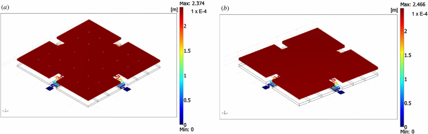
Figure 4. FEM simulation of the vibration of the movable plate with a thickness and a resonance frequency of (a) 30 µm and 875 Hz, (b) 50 µm and 678 Hz. It is observed that the movable plate vibrates without deformation.
Download figure:
Standard image4. Fabrication
The MEMS variable capacitors with two cavities were fabricated on top of the silicon substrate using surface micromachining. A cross-sectional view of the fabrication processes is shown in figure 5. The fabrication starts with etching 3 µm deep rectangular trenches into a silicon wafer at locations corresponding to the locations of anchors of the movable plates and bonding tabs using a reactive ion etch (RIE) system. The patterned wafers were then thermally oxidized to grow 1 µm thick SiO2 layer for insulation. Thin layers of Cr and Au were deposited by sputtering. Cr serves as an adhesion layer for Au. The Au layer was patterned to form the bottom plates, bottom and top electrodes, trace lines and the seed layer at locations corresponding to anchors of the movable plates and bonding tabs (figure 5(a)). Another Au layer was electroplated inside a photoresist mold to create stoppers. Thin layers of SiO2 and Si3N4 were then sputter deposited and patterned to the shape of the bottom plates to enhance the dielectric property of the capacitors and to insulate the Au stoppers (figure 5(b)). A thick photoresist sacrificial layer was patterned with a height of 30 µm serving as a mold for creating the anchors of the movable plate and bonding tabs. Ni was electroplated inside the mold to form the anchors and bonding tabs. The second seed layer of Cr and Au was similarly sputter deposited (figure 5(c)). A photoresist mold was patterned on top of the second seed layer to create the movable plates with serpentine shape suspension beams. Ni was electroplated inside this photoresist mold for a thickness of 5 µm (figure 5(d)). The movable plate thickness was then increased without changing the thickness of suspension beams by electroplating another 25 µm thick Ni in another photoresist mold with only features of movable plates (figure 5(e)). In addition, one more photoresist mold was patterned for only the bonding tabs in order to electroplate 1 µm thick In for bonding purpose (figure 5(f)). Finally, all of the photoresist molds on top of the second seed layer were removed by flushing with acetone, isopropanol and DI water very carefully without attacking the sacrificial layer. The second seed layer was removed by wet etching of Au and Cr. The photoresist sacrificial layer was released in hot photoresist stripper bath. Ultrasonic agitation was added in this step to help removal of the sacrificial layer under the movable plates. The Cr layer on the bottom substrate serving as the first seed layer was finally etched away (figure 5(g)).
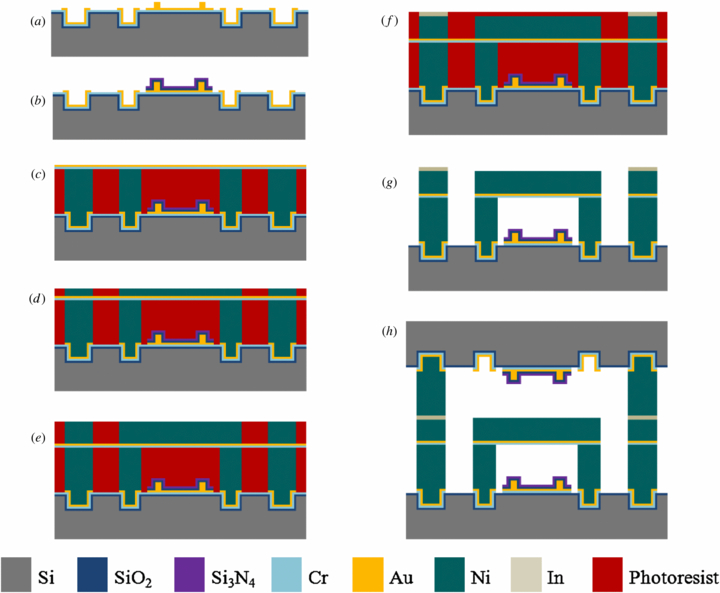
Figure 5. Side view schematics of the fabrication processes flow for the two-cavity MEMS variable capacitor.
Download figure:
Standard imageAnother substrate with only fixed plates and dielectric layers was prepared by the same microfabrication procedures. This substrate will be used to create the top capacitive cavity. The bonding tabs on this substrate were similarly electroplated with Ni and In with thicknesses of 30 µm and 1 µm, respectively. To create the two-cavity variable capacitor, the two substrates were diced into small dice, each containing one device. The bonding tabs on the two substrates were then aligned under the microscope and on top of a hotplate. Once the two substrates were aligned, they were heated at 200 °C in order to melt the two indium layers and form a strong bond between them after the device is cooled down. This temperature was found to give the best bonding quality without affecting the structure integrity (figure 5(h)).
5. Results
The fabrication processes of each layer forming the two-cavity MEMS variable capacitors were optimized, and the initial prototypes were successfully fabricated. The fabricated nickel electroplated MEMS power harvesting device has a movable plate with a thickness of 30 µm, suspension beams with a total length, width and thickness of 1040 µm, 15 µm and 5 µm, respectively, and the two air cavities each has a depth of 30 µm. SEM micrographs of the resulting power harvesting devices with one cavity and two cavities are shown in figures 6 and 7. The micrographs display clearly that the movable plate is suspended with a flat surface. It is also clear from the micrographs that the two air gaps have similar heights as designed.

Figure 6. SEM micrographs of MEMS variable capacitors without bonding the second cavity: (a) SEM of distant view of two 2 × 2 mm2 MEMS capacitive plates with 30 µm gap in a 1 × 4 array, (b) a distant view of a single device with an air gap, suspension beams and a movable plate with thicknesses of 30, 5, 30 µm, respectively, (c) a magnified view of a suspension beam with width, length and thickness of 15, 1040 and 5 µm.
Download figure:
Standard image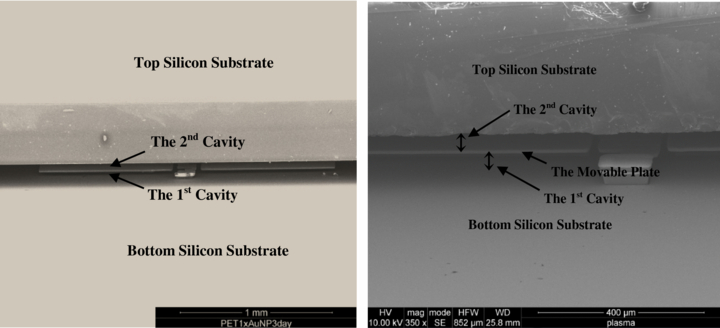
Figure 7. SEM micrographs of the 2 × 2 mm2 MEMS variable capacitor with two cavities.
Download figure:
Standard imageInitial characterization was performed to confirm the successful suspension of the electroplated nickel movable plate. The capacitance of MEMS variable capacitor Cvar without bonding the second cavity was measured as a function of the voltage applied. The dynamic measurement of capacitance variation was achieved by measuring the phase shift in an RCvar circuit. The pull-down effect was observed at around 13 V (figure 9(a)), which verifies the FEM modeling results. The device was then fixed to a vibration stage for excitation and wire bonded to an electrical testing circuit (figure 8) for measuring frequency sweeps at fixed excitation amplitude. The collection of data is accomplished with a data acquisition board (NI USB-6218 DAQ) controlled by a PC using Labview. The MEMS variable capacitor was charged by a 9V dc battery as an input voltage Vin. The RMS voltage across either one of 5 MΩ load resistors was measured as function of frequency under relatively low and constant sinusoidal excitation amplitude. A peak RMS voltage of 287 mV was observed around 900 Hz under a peak-to-peak sinusoidal excitation voltage Vp-p of 700 mV to the shaker (figure 9(b)). A time-domain plot of the output voltage across the load resistor under the sinusoidal excitation voltage Vp-p of 700 mV and a constant frequency of 900 Hz is shown in figure 9(c). The output power against various excitation frequencies was calculated from the measured RMS voltage across the load resistor as the frequency sweeps (see figure 9(d)).
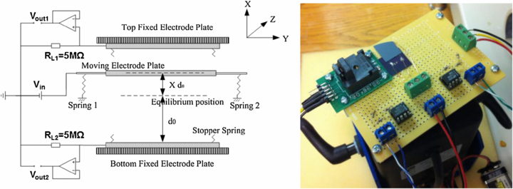
Figure 8. Electrical testing circuit and experimental PCB test board for characterization of the MEMS variable capacitor.
Download figure:
Standard image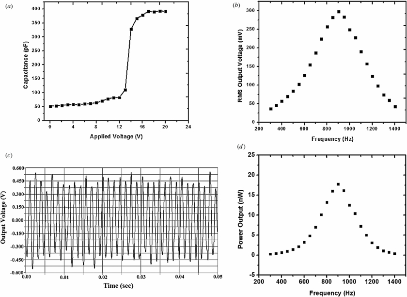
Figure 9. Characterization of a single-cavity MEMS variable capacitor: (a) the change of capacitance with increasing applied voltage, pull-down effect is observed at around 13V. (b) The RMS voltage across a 5 MΩ load resistor as a function of frequency under sinusoidal excitation voltage Vp-p of 700 mV, (c) output voltage across the load resistor in time domain under sinusoidal excitation voltage Vp-p of 700 mV and frequency of 900 Hz, (d) power output from one cavity of the capacitor as a function of frequency under sinusoidal excitation voltage Vp-p of 700 mV.
Download figure:
Standard imageIn this study, we have identified the ranges of the forcing frequencies and amplitudes for which power generation on the order of µW is achieved by Matlab simulation. By tracking the change of the electric charges on the capacitors, we are able to compute the current, and hence the power that can be achieved by the power harvester. We also have a numerical program that can calculate the harvested power for given geometric design and for given vibration amplitude and frequencies. Extensive testing and analyses of dynamic behaviors and optimization of power generation on two-cavity MEMS variable capacitor under various excitation conditions will be reported in a future paper.
6. Conclusions
We have designed and fabricated a 2 × 2 mm2 MEMS variable capacitor for scavenging energy from vibration in environment using electrostatic mechanism. The advantages of this novel design in the use of two capacitive cavities were demonstrated by using time-domain simulation in Matlab program. The model showed that the two-cavity design has achieved higher average power than single-cavity devices under a wide range of external forcing frequency and amplitude. The FEM model was used to determine the stiffness of the designed movable plate and demonstrate vibration of the movable plate without deformation or breaking. The characterizations of single-cavity variable capacitors were performed to explore the dynamic behaviors and power generation. The output voltage and power generation will be optimized with an improved power extraction circuit in the future.
Acknowledgment
This work was sponsored by National Science Foundation under Grant No CMMI-0900727.