
Abstract
The output of a piezoelectric nanogenerator (NG) fabricated using ZnO nanowire arrays is largely influenced by the density of the surface charge carriers at the nanowire surfaces. Adsorption of gas molecules could modify the surface carrier density through a screening effect, thus, the output of the NG is sensitive to the gas concentration. Based on such a mechanism, we first studied the responses of an unpackaged NG to oxygen, H2S and water vapor, and demonstrated its sensitivity to H2S to a level as low as 100 ppm. Therefore, the piezoelectric signal generated by a ZnO NWs NG can act not only as a power source, but also as a response signal to the gas, demonstrating a possible approach as a self-powered active gas sensor.
Export citation and abstract BibTeX RIS
A correction was made to this article on 15 May 2013. Additional author email added.
1. Introduction
Nanogenerators (NGs) based on the piezoelectric [1–3], triboelectric [4] or pyroelectric [5] effect, which can convert trace energy in the environment into electric energy, have performed as an efficient energy source for nanodevices and nanosystems. Self-powered nanosystems have been proved viable in self-powered pH sensors [6], UV sensors [7], self-charging power cells [8], small liquid crystal displays [9], commercial laser diodes [10], etc. Most recently, a new type of self-powered nanosystem, named as an active sensor, has been demonstrated by treating the output electric signal from NGs as either a power source or sensing signal in response to the change in environment, such as ambient wind velocity detectors [11], automobile speedometers [12] and magnetic sensors [13]. Among various NG-based active sensors, ZnO nano/micro-wires have been intensively investigated because of their semiconducting and piezoelectric coupling properties [14, 15]. Taking a ZnO-based active photodetector as an example, ZnO nanowires (NWs) generate different piezoelectric output under different intensities of UV illumination because the carrier density is significantly influenced by the intensity of UV illumination [7, 16].
Because of their semiconducting property, ZnO one-dimensional nanostructures are considered as extremely sensitive and fast responsive materials for gas sensing due to their large surface-to-volume ratio and surface adsorption activity [17–19]. If the gas sensing and piezoelectric properties of ZnO NWs NG can be coupled into a single physical process then a new type of self-powered active gas sensor can be realized through its surface-state-dependent piezoelectric output.
In this paper, we study the output response of an unpackaged NG to gases in which the NG is placed, aiming to explore the mechanism of coupling the free-carrier screening effect with piezoelectric properties. Our study demonstrates that the ZnO NW NGs can act as self-powered sensors for actively detecting various gases without requiring external power. Our results can stimulate a possible new direction for the development of the next generation of gas sensors and will further expand the scope for self-powered nanosystems.
2. Experimental section
The design of the NG is shown in figure 1(a). The device is composed of three major components: the ZnO NW array, Ti foil and Al layer as electrodes, Kapton boards as bracing frames. An optical image of a NG, presented in the inset of figure 1(a), indicates that the NG has a length of 3 cm and a width of 3 cm, and also shows that the device is very flexible, a good feature making it efficiently convert external compressive strain into an electrical signal [20, 21]. A brief fabrication process can be described as follows. Pre-cleaned Ti substrates are deposited with ZnO seeds. Then ZnO NW arrays are grown on the surface of Ti foils by the simple wet-chemical method described below. ZnO NW arrays were prepared by a two-step process. Zinc acetate dehydrate (Zn(CH3COO)2⋅2H2O) was dissolved in ethanol with a concentration of 10 mM. A droplet of solution was coated onto pre-cleaned Ti substrates, then blown dry with nitrogen gas. The coated substrates were annealed at 350 ° C for 20 min in air to yield a layer of ZnO seeds. Then, ZnO NWs arrays were synthesized via a wet-chemical route in 200 ml of equimolar (50 mM) aqueous solution of Zn(NO3)2⋅6H2O and HMTA in a reaction flask at 90 ° C. The Ti substrate coated with ZnO seed layers was immersed into the aqueous solution. After 2 h, the substrates were removed from the solution, rinsed with deionized water, and dried at room temperature. Figures 1(b) and (c) are the scanning electron microscopy (SEM) images of the top-view and cross-sectional view of the ZnO NW arrays, respectively, revealing their diameters of ∼500 nm and lengths of ∼5 μm. A high-resolution transmission electron microscopy (HRTEM) image and the corresponding selected area electron diffraction (SAED) pattern taken from the tip region of a ZnO NW are presented as figure 1(d), indicating that the ZnO NW is structurally uniform and single crystalline with a length direction along the c-axis. In this device, Ti foil acts as the substrate for the ZnO NWs arrays and as the conductive electrode that collects the piezoelectric voltage signal generated by ZnO NWs when being deformed by external compression. As the counter-electrode, a sheet of flexible aluminum foil (0.05 mm thick) is positioned on top of the ZnO NW arrays. Two terminal copper leads were glued with silver paste on the Ti foil and Al foil for electrical measurements. The finished device is fixed between two sheets of Kapton board. A gas flow chamber was used as the test container. The NG and the manipulator, producing a constant strain, were fixed inside of the chamber. The concentration of test gases was controlled exactly by using gas flow meters. The piezoelectric output voltage was independently monitored by a low-noise preamplifier (Model SR560, Stanford Research Systems).
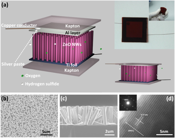
Figure 1. Structural design of the NG proposed for our study. (a) Schematic diagram showing the structural designal of the NG; the inset is a photograph of a typical NG. (b) SEM image of ZnO NW arrays grown on Ti foil in a top view. (c) SEM image of ZnO NW arrays in a cross-sectional view. (d) HRTEM and SAED pattern taken from the tip region of a ZnO NW.
Download figure:
Standard image3. Results and discussion
It is known that the as-grown ZnO NWs have a high density of point defects, which serve as n-type carriers for the measured conductivity. Previous experiments show that functionalizing the ZnO NW surfaces with a p-type polymer can dramatically increase the output of the NG because of its capture of n-type carriers at the surface, thus, reducing the screening effect of the free carriers on the piezoelectric polarization charges [22]. Alternatively, the free-carrier density at the surfaces of ZnO NWs is affected by oxidizing or reducing gas adsorbed on the surface, which greatly changes the screening of the piezoelectric polarization charges at the interface by the free carriers, thus affecting the piezoelectric output of the NG. From previous theoretical and experimental works, the change in free-carrier density affects the intrinsic potential of the Schottky contact or p–n junction in piezoelectronic devices [23, 24].
In fact, NGs under the same strain have different piezoelectric outputs when placed in different gases. The NGs have two functions: one is as an energy source because the NG can produce piezoelectric output power; the other is a sensor function because the output of NG is a measure of surface adsorbed gas molecules. Each gas sensing cycle can be described as follows. At the very beginning, the NG is in a natural state without compressive or tensile strain, and no piezoelectric field is produced along ZnO NWs. When it is exposed to oxygen, for example, the oxygen molecules can be adsorbed on the surface of ZnO NWs by capturing their free electrons and forming oxygen ions (O−2, O− and O2−) [25–27]. This process can reduce the charge-carrier density and increase the thickness of the depletion layer in ZnO NWs, as shown in the figure 2(a). When the device is under a compressive strain, a piezoelectric field is created along the NWs. Free electrons in the conduction band tend to flow and screen the positive ionic piezoelectric charges at one end, while leaving the negative ionic piezoelectric charges alone [28]. When exposed to oxygen, the density of free electrons at the NW surface is reduced and the depletion layer is widened, resulting in an increased piezoelectric output (figure 2(b)).
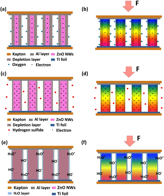
Figure 2. The working mechanism of the NGs driven by compressive strain. (a) Schematic illustration of the charge-carrier density and thickness of the depletion layer in ZnO NWs without compression in oxygen. (b) Schematic of the piezoelectric output of NGs in oxygen under mechanical deformation. (c) Schematic illustration of the charge-carrier density and thickness of the depletion layer in ZnO NWs without compression in hydrogen sulfide. (d) Schematic of the piezoelectric output of NGs in hydrogen sulfide under mechanical deformation. (e) Water layer on the surface of ZnO NWs when exposed to water vapor. (f) Schematic of the piezoelectric output of NGs in water vapor under mechanical deformation. The color code is used here to qualitatively illustrate the distribution of the piezoelectric potential in the nanowires.
Download figure:
Standard imageWhen the device is exposed to hydrogen sulfide gas with a strong reducing characteristic, the oxygen ions adsorbed on the surface of ZnO NWs will react with H2S molecules and release the captured electrons flowing back into the conduction band of ZnO NWs ( ) [29]. This process can increase the carrier density and reduce the thickness of the depletion layer in ZnO NWs, as shown in figure 2(c). So, upon exposure to H2S, the screen effect of free electrons is strong and the piezoelectric output voltage of the NGs is lowered, as shown in figure 2(d).
The humidity sensing of NGs is related to a water-adsorption process. When the device is exposed to humidity, water vapor is chemisorbed on the surface of ZnO NWs initially. In this case, hydroxyl (OH−) ions can be formed on the surface and proton transfer occurs among the hydronium (H3O+) [30]. Usually, only one monolayer of water covers the NW surface at around 20 RH%, and physisorbed layers are formed with increasing humidity (figure 2(e)) [30]. H3O+ appears in the physisorbed water and the proton of water molecules with H3O+ ions is released to the neighboring water molecules, and likewise to next ones. So H3O+ can be regarded as charge carriers of H2O-adsorbed ZnO NWs. Under compressive deformation, both H3O+ in the physisorbed water layer and the free electrons inside the ZnO NWs could have directional movement to partially screen the piezoelectric polarization charges in the NWs, and the piezoelectric output voltage of NGs is lowered (figure 2(f)).
As discussed above, the free-carrier density, no matter whether they are free electrons inside ZnO NWs or H3O+ in the water layer, plays a crucial role in affecting the output of the NG. Oxygen molecules decrease the carrier density by capturing free electrons in NWs; H2S molecules increase the carrier density by desorbing oxygen molecules from the surface of NWs; water vapor also increases the carrier density by covering the surface of NWs with a water layer containing H3O+ ions. Such a change of charge-carrier density can be directly demonstrated by the resistance of the ZnO NWs. Figure 3 shows the I–V curves of one NG in different gases (1.01 × 10⁵ Pa) without deformation at room temperature. There is typical metal–semiconductor–metal (M–S–M) structure in our devices (Al–ZnO–Ti). The nonlinear I–V characteristic is caused by the asymmetric Schottky barrier heights formed between ZnO NWs and two metal electrodes [23]. Compared with the curve of one NG in dry air, the I–V curves shift downwards when the device is exposed to oxygen and upwards in H2S and water vapor. The changes of resistance further confirm the changes of carrier density in ZnO NWs upon exposure to the various gases discussed above. As ZnO NWs have different charge-carrier density in different gases, the piezoelectric output of NGs influenced by carrier density also contains the gas sensing information.

Figure 3. Typical I–V characteristics of a NG in different gases (1.01 × 10⁵ Pa) without deformation at room temperature. The contact at the Ti–ZnO interface has the highest Schottky barrier.
Download figure:
Standard imageThe dependence of the NG on the gas atmosphere can be a potential approach for gas sensing. The piezoelectric output voltage of one device with a size of 3 cm × 3 cm under the same applied strain 0.012% at the same frequency (0.4 Hz) at room temperature under 1.01 × 10⁵ Pa is measured in dry air, pure oxygen, water vapor (85 RH%) and H2S (1000 ppm in air). The voltage response of the device in different gases is shown in figure 4. When the device is in dry air, the piezoelectric output voltage of the NGs induced by the compressive strain is 0.45 V (figure 4(a)). In pure oxygen, the piezoelectric output voltage increased to 0.7 V (figure 4(b)). ZnO NWs in pure oxygen will absorb more oxygen molecules than in dry air, resulting in a lower free electron density and thicker depletion layer of ZnO NWs. Upon exposure to H2S (1000 ppm in air) and water vapor (85 RH%), the piezoelectric output voltage decreases to 0.198 V (figure 4(c)) and 0.35 V (figure 4(d)), respectively. The output current of the device is shown in figure S1 (available at stacks.iop.org/Nano/24/225501/mmedia). Similar to the traditional definition of sensitivity of a gas sensor ( , where Ra and Rg are the resistance of the sensors in air and test gas, respectively) [31], the sensitivity S of the NGs in the same deformation conditions can simply be defined as:
where Va and Vg are the piezoelectric output voltage in dry air and test gas, respectively. The sensitivity S in pure oxygen, water vapor (85 RH%) and H2S (1000 ppm in air) is −35.7, 28.6 and 127.3%, respectively.
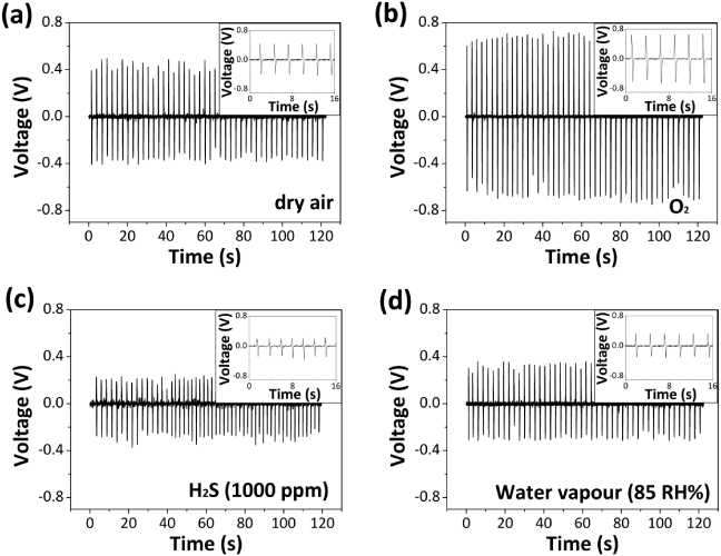
Figure 4. Voltage response of one NG that was repeatedly compressed by an applied strain of 0.012% with a strain rate 0.06% s−1 at a frequency of 0.4 Hz in (a) dry air, (b) oxygen, (c) 1000 ppm H2S and (d) 85 RH% water vapor. All the measurements are performed at room temperature and under 1.01 × 10⁵ Pa.
Download figure:
Standard imageThe piezoelectric output voltage of NGs is related to the concentration of the test gases, as shown in figure 5(a). The piezoelectric output voltage of NGs decreases as the concentration of H2S increases. Upon exposure to 100, 250, 400, 550, 700, 850 and 1000 ppm H2S, the piezoelectric output voltage of NGs under a constant applied strain (0.012%, 0.4 Hz) is about 0.398, 0.360, 0.289, 0.251, 0.203, 0.202 and 0.198 V, respectively. The sensitivity S against 100, 250, 400, 550, 700, 850 and 1000 ppm H2S is about 13.1, 25.5, 55.7, 79.3, 121.7, 122.8 and 127.3%, respectively (figure 5(b)). With the increase of the concentration of H2S, more H2S molecules can cause more oxygen molecules to be desorbed from the surface of ZnO NWs, reducing the thickness of the charge depletion layer and increasing the nanowire conductivity. It should be pointed out that saturation of the sensitivity of NGs can be observed if the concentration of H2S is higher than 700 ppm. Such a saturation of sensitivity is similar to that in traditional gas sensors, arising from the competition between the adsorption sites versus the concentration of target gas [32].
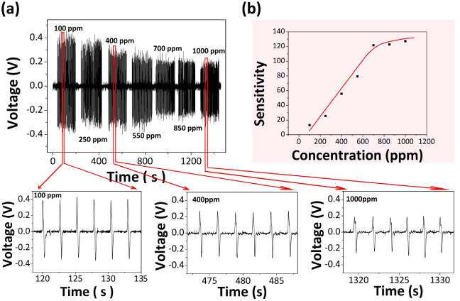
Figure 5. (a) The output voltage of NGs in 100, 250, 400, 550, 700, 850 and 1000 ppm hydrogen sulfide at room temperature and 1.01 × 10⁵ Pa. The compressive strain applied to NG is 0.012%, 0.4 Hz. (b) The dependence of sensitivity S on the concentration of H2S.
Download figure:
Standard imageIn order to verify that the change of NG output voltage is indeed caused by the different gases, a control experiment is performed on a NG fully sealed with epoxy, as shown in figure S2 (available at stacks.iop.org/Nano/24/225501/mmedia). As schematically shown in figure S2(a), the NG is completely sealed in a large amount of epoxy, including ZnO NWs, metal electrodes and Kapton substrates, and no gas molecules can contact with ZnO NWs. Under the same applied strain (0.012%, 0.4 Hz) in dry air, pure oxygen, hydrogen sulfide (1000 ppm) and water vapor (85 RH%), the piezoelectric output voltage of the epoxy-sealed NGs stays the same, as shown in figure S2(b). The piezoelectric output voltage of the epoxy-sealed NGs does not change with varying external atmosphere, and the output voltage is ∼0.17 V in all test gases. These results further confirm that the piezoelectric output of NGs in figure 4 is influenced by the external gas environment. The NG can be a single source of output power, as has been verified as shown in figure S3 (available at stacks.iop.org/Nano/24/225501/mmedia). Through the bridge rectifier, an AC signal can be produced by the NG and converted into a DC signal, which can be used directly to charge a nanostructure-based lithium ion battery [33–35].
4. Conclusions
In summary, we have studied the response of an NG to the gas environment in which it is placed. The data can be understood by considering the effect of adsorbed molecules on the density of the free carriers in the NWs. Also, we demonstrated the first applications of NGs as self-powered gas sensors. The unpackaged NGs showed different outputs in different gas environments. The piezoelectric signal generated by ZnO NWs was both the power source of this self-powered device and the gas sensor due to the different screening effectiveness of free electrons on the piezoelectric charges in different gases. A new type of active gas sensor is demonstrated for self-powered nanosystems.
Acknowledgments
This work was partly supported by the Beijing Institute of Nanoenergy and Nanosystems, the Fundamental Research Funds for the Central Universities (Grant No. lzujbky-2013-35), the Knowledge Innovation Program of the Chinese Academy of Sciences (Grant No. KJCX2-YW-M13), and the National Natural Science Foundation of China (51102041 and 11104025).